
Utilizing Sidewall Spacer Features to Form Magnetic Tunnel Junctions in an Integrated Circuit

a technology of integrated circuits and sidewall spacers, which is applied in the direction of electrical equipment, semiconductor devices, galvano-magnetic devices, etc., can solve the problems of etching byproducts, difficult or impractical to remove, and particularly problematic redeposition of byproducts

Inactive Publication Date: 2008-09-04
GLOBALFOUNDRIES INC
View PDF10 Cites 27 Cited by
  • Summary
  • Abstract
  • Description
  • Claims
  • Application Information

AI Technical Summary

Benefits of technology

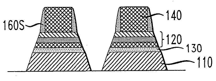
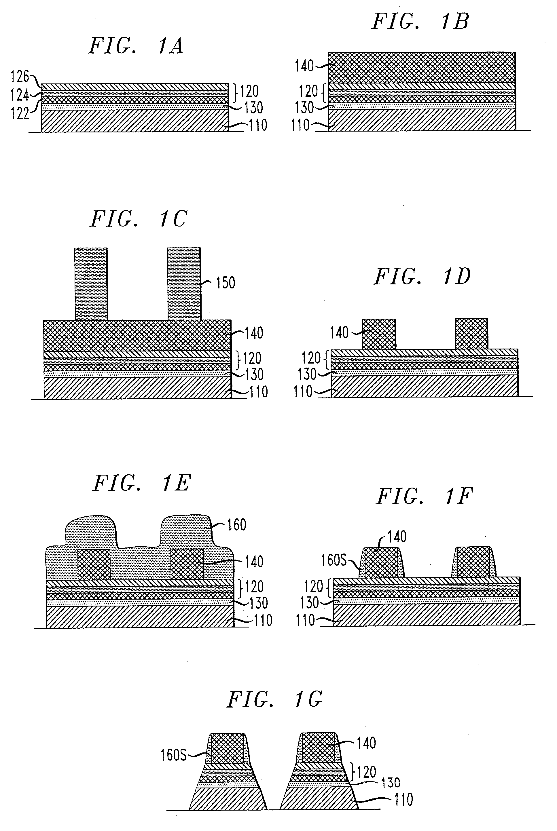
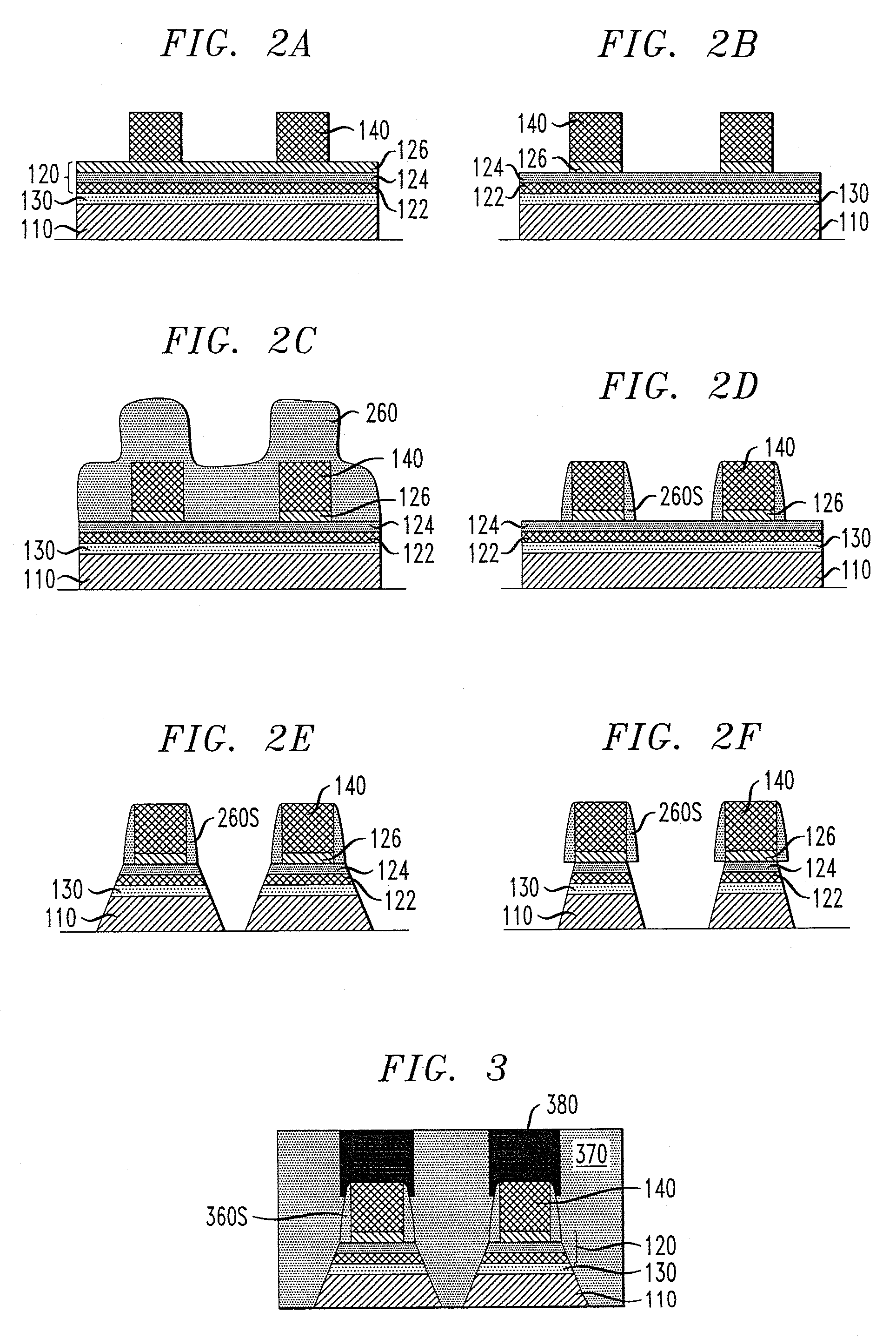
The present invention provides a novel method for reliably and reproducibly forming MTJs (magnetic tunnel junctions) in integrated circuits. This is achieved, at least in part, by using sidewall spacer features during the processing of the film stack. These features create a characteristic tapered masking feature and an encapsulating layer for protecting a portion of the film stack during subsequent processing steps. Additionally, the sidewall spacer features may be left in place and used as vertical contacts to higher levels of metallization. This method reduces redeposition of etching byproducts, resulting in improved MRAM processing yield.

Problems solved by technology

Such byproduct redeposition is especially problematic in producing MRAM circuitry.
The etching byproducts formed when etching MTJ features are extremely difficult or impractical to remove without using methods that also cause harm to the sensitive film stack that makes up the etched device itself.
The difficulty, however, lies in finding a reliable and reproducible way of forming such a taper.
However this balancing process is complex, and the balance of these three components is highly sensitive to the condition of the etch tool.
Nevertheless, because of the possibility of damage to the underlying film stack, the physical sputtering of the masking layer is usually limited.
This frequently means that lower reaches of the masking layer cannot be tapered sufficiently.
As a result, the redeposition of etching byproducts is frequently still problematic when subsequently etching the remainder of the film stack.

Method used


Image

  • Utilizing Sidewall Spacer Features to Form Magnetic Tunnel Junctions in an Integrated Circuit
  • Utilizing Sidewall Spacer Features to Form Magnetic Tunnel Junctions in an Integrated Circuit
  • Utilizing Sidewall Spacer Features to Form Magnetic Tunnel Junctions in an Integrated Circuit

Examples


Embodiment Construction

[0017]This invention will be illustrated herein in conjunction with exemplary methods for forming MTJ features in integrated circuitry. It should be understood, however, that the invention is not limited to the particular materials, film layers and processing steps shown and described herein. Modifications to the illustrative embodiments will become apparent to those skilled in the art.

[0018]Particularly with respect to processing steps, it is emphasized that the descriptions provided herein are not intended to encompass all of the processing steps which may be required to successfully form a functional device. Rather, certain processing steps which are conventionally used in forming integrated circuit devices, such as, for example, wet cleaning and annealing steps, are purposefully not described herein for economy of description. However one skilled in the art will readily recognize those processing steps omitted from this generalized description. Moreover, details of the process s...


PUM


Abstract

Novel methods for reliably and reproducibly forming magnetic tunnel junctions in integrated circuits are described. In accordance with aspects of the invention, sidewall spacer features are utilized during the processing of the film stack. Advantageously, these sidewall spacer features create a tapered masking feature which helps to avoid byproduct redeposition during the etching of the MTJ film stack, thereby improving process yield. Moreover, the sidewall spacer features may be used as encapsulating layers during subsequent processing steps and as vertical contacts to higher levels of metallization.

Description

CROSS-REFERENCE TO RELATED APPLICATION(S)[0001]This application is a continuation of pending U.S. application Ser. No. 11 / 333,997 filed on Jan. 18, 2006, the disclosure of which is incorporated herein by reference.FIELD OF THE INVENTION[0002]This invention relates generally to integrated circuits, and more particularly to techniques for utilizing sidewall spacer features to form magnetic tunnel junctions in integrated circuits.BACKGROUND OF THE INVENTION[0003]Magnetic memory devices, such as magnetic random access memory (MRAM) devices, use magnetic memory cells to store information. Information is stored in a magnetic memory cell as the orientation of the magnetization of a free layer in the magnetic memory cell as compared to the orientation of the magnetization of a fixed or pinned layer in the memory cell. The magnetization of the free layer may be oriented parallel or anti-parallel to the fixed layer, representing either a logic “0” or a logic “1.” One type of memory cell, a ma...

Claims


Application Information

Patent Timeline
Patent Type & Authority Applications(United States)
IPC IPC(8): H01L43/00H01L43/12H10N50/01
CPCH01L43/12H01L27/222H10B61/00H10N50/01
Inventor ASSEFA, SOLOMONGAIDIS, MICHAEL C.KANAKASABAPATHY, SIVANANDAHUMMEL, JOHN P.ABRAHAM, DAVID W.
Owner GLOBALFOUNDRIES INC
Learn More