Optical Circuits and Circuit Elements and Methods of Forming Same

a technology applied in the field of optical circuits and circuit elements, can solve the problems of not working at frequencies beyond the far infrared, the scaling of circuit components conventionally used in the rf and lower frequencies, and the inability to straightforwardly scale down metallic materials to the infrared and optical frequencies, etc., to achieve positive effective “inductance”, more flexibility, and more degree of freedom

Active Publication Date: 2008-09-04
THE TRUSTEES OF THE UNIV OF PENNSYLVANIA
View PDF6 Cites 3 Cited by
  • Summary
  • Abstract
  • Description
  • Claims
  • Application Information

AI Technical Summary

Benefits of technology

[0046]In this case, the real part of ∈ is a positive quantity; thus Zsph in Eq. (6) is capacitive, while having a resistive part that is related to the imaginary part of permittivity. The impedance of the outside fringe is always capacitive because the permittivity of the outside region can be assumed to be positive. Thus, the equivalent nano-circuit for a non-plasmonic nanosphere, which is small compared with the optical wavelength, can be shown as in the bottom left part of FIG. 1. Here the equivalent circuit elements can be expressed in terms of parameters of the nanospheres as follows:
[0047]In this case, the sphere can be made of a plasmonic material, such as noble metals in the visible or IR band (e.g., Ag, Au), which results in the real part of the permittivity of the material having a negative value in these frequency bands. Therefore, the equivalent impedance of the nanosphere (Eq. 6) can be “negatively capacitive”, which implies that at any given frequency for which Re[∈]<0, the equivalent capacitance is “negative”. This can be interpreted as a positive effective “inductance”, as discussed in A. K. Sarychev, D. A. Genov, A. Wei, and V. M. Shalaev, Proceedings of SPEE, Complex Mediums IV, 81 (2003); G. V. Eleftheriades, A. K. Iyer, and P. C. Kremer, IEEE Trans. Microwave Theory Tech, 50, 2702 (2002); and N. Engheta, N. Bliznyuk, A. Alù, A. Salandrino, Dig. USNC-URSI National Radio Science Meeting, Monterey, Calif., 276 (2004). Therefore, the equivalent circuit for the case of optical wave interaction with a plasmonic nanosphere is represented in the bottom right of FIG. 1.
[0048]The equivalent circuit element for a sphere formed of plasmonic material can be calculated as:
[0049]Accordingly, a small nanosphere excited by an optical (or infrared) signal may effectively behave as a “nano-capacitor” or a “nano-inductor”—analogous to the respective circuit elements in an electrically conductive circuit—at the optical frequency, if the sphere is made of non-plasmonic or plasmonic materials, respectively. The imaginary part of the material permittivity can provide an equivalent nano-resistor—these resistors can be either a plasmonic or nonplasmonic particles as long as they have some non-zero imaginary part in the permittivity. Unlike the conventional design for an inductor in the lower frequency regimes, where the inductor is usually in the form of “wound wires”, the present inductors operating in the optical and infrared regimes is made of a simple geometry consisting of plasmonic materials. In other words, instead of winding wires with dimensions much smaller than the optical wavelength, here the plasmonic characteristics of natural noble metals provide an effective inductance, whose value can be designed by properly selecting the size, shape, and material contents of the nanostructure. Modulation of these parameters can result in achieving the desired effective inductance.
[0050]The described circuit elements for the optical and infrared regimes provide new possibilities for miniaturization of circuits. Conventional circuits in the RF and lower frequencies, which relying on the conduction current circulating in metallic wires along the lumped elements, cannot be straightforwardly scaled down to the infrared and optical frequencies. At these high frequencies, the conducting metallic materials behave quite differently. However, introducing plasmonic and non-plasmonic nanoparticles as basic elements of optical nanocircuits, in which effectively the “displacement” current can similarly “circulate”, can now provide for analogous functionalities at the optical frequencies. One can essentially have the three basic circuit elements, i.e., nano-inductor, nano-capacitor, and nano-resistor, operating in the optical frequency, which form the building blocks for the design of more complex circuits at these wavelengths.
[0051]For any given wavelength and specific material, the values of these optical circuit elements depend directly on the size and shape of the particles, e.g., for the nanosphere, this would be calculated from the radius. However, if one wants to have more flexibility (i.e., more degrees of freedom) in their design, one can use nanoparticles with different geometries, e.g., ellipsoidal nanoparticles, where there are three geometrical parameters, corresponding to the three axes that can be manipulated to achieve the desired result, whether inductance, capacitance, or resistance.

Problems solved by technology

It should be pointed out that a mere scaling of the circuit component concepts conventionally used in the RF and lower frequencies may not work at frequencies beyond the far infrared.
However, the metallic materials cannot be straightforwardly scaled down to the infrared and optical frequencies because at this size the conducting metallic materials behave quite differently.

Method used


Image

  • Optical Circuits and Circuit Elements and Methods of Forming Same
  • Optical Circuits and Circuit Elements and Methods of Forming Same
  • Optical Circuits and Circuit Elements and Methods of Forming Same

Examples


example 1

Nanoinductor Optical Circuit Element

[0059]A three dimensional particle in the shape of a sphere having a radius R=30 nm is formed using silver. At the wavelength λ0=633 nm, the permittivity of silver is known to be ∈Ag=(−9+i0.53)∈0 (See P. B. Johnson, and R. W. Christy, Phys. Rev. B, 6, 4370 (1972)). From Eq. (8), the particle is determined to exhibit nanoinductance Lsph=7.12 femtoH upon exposure to light having a wavelength λ0=633 nm.

example 2

Nanocapacitor Optical Circuit Element

[0060]A three dimensional particle in the shape of a sphere having a radius R=30 nm is formed using Au2S. At the wavelength λ0=633 nm, the permittivity of ∈Au2S=5.44∈0. The nanocapacitance exhibited by the sphere is determined to be Csph=4.53 attoF upon exposure to light having a wavelength λ0=633 mm.

example 3

Left Handed Nanoscale Transmission Line

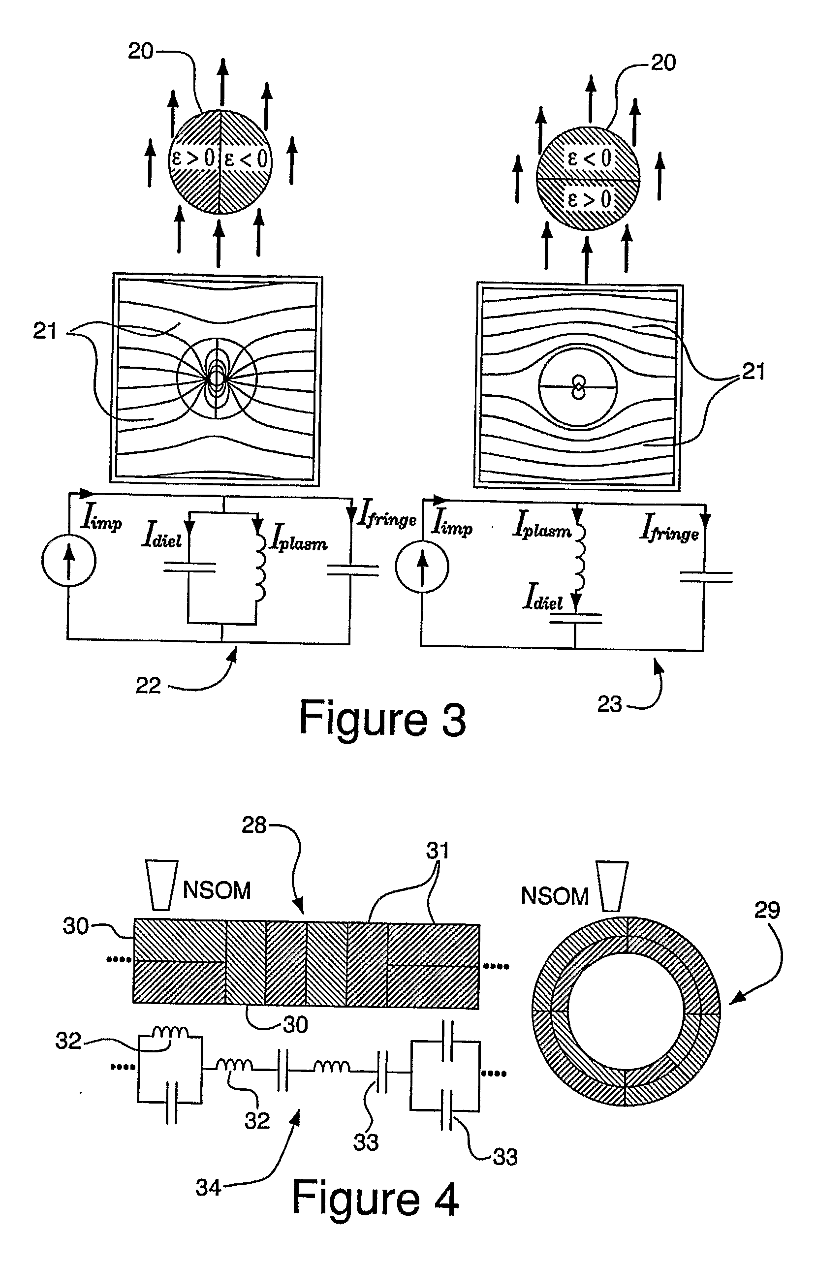
[0061]A nanocircuit in the form of a left-handed (LH) nanoscale transmission line is formed by depositing a first uniform layer of non-plasmonic nanoparticles onto a substrate. Each non-plasmonic nanoparticle is separated from an adjacent non-plasmonic nanoparticle by a distance substantially small enough to permit optical coupling. This separation distance is maintained throughout the layer. A uniform layer of plasmonic nanoparticles is then elaborated over the first uniform layer of non-plasmonic nanoparticles. As with the first uniform layer, each plasmonic nanoparticle is separated from an adjacent plasmonic nanoparticle by a distance substantially small enough to permit optical coupling. Also, the separation distance is maintained throughout the layer. To this layer of plasmonic nanoparticles, another uniform layer of non-plasmonic nanoparticles is deposited onto the uniform layer of plasmonic nanoparticles. The properties of this layer be...


PUM


Abstract

Circuits and circuit elements adapted to function at optical or infrared frequencies are made from plasmonic and/or nonplasmonic particles disposed on a substrate, where the plasmonic and nonplasmonic particles have respective dimensions substantially smaller than a wavelength of an applied optical or infrared signal. Such particles are deposited on a substrate in a variety of shapes and sizes from a variety of plasmonic and/or nonplasmonic materials so as to form resistors, capacitors, inductors and circuits made from combinations of these elements.

Description

CROSS-REFERENCE TO RELATED APPLICATIONS[0001]The present patent application claims the benefit of the filing date of U.S. Provisional Patent Application Ser. No. 60 / 581,016, Jun. 18, 2004, which is hereby incorporated by reference in its entirety.STATEMENT OF FEDERALLY SPONSORED RESEARCH[0002]The U.S. government may have certain rights in the invention described herein, which was made in part with funds from the U.S. Defense Advanced Research Projects Agency (DARPA) Grant number HR0011-04-P-0042 and the U.S. Air Force Office of Scientific Research (AFOSR) Grant number F49PRE-03-1-0438.FIELD OF THE INVENTION[0003]The present invention relates to circuits and circuit elements that operate in the IR and visible regimes using plasmonic and non-plasmonic nanostructures, and the methods for forming the same.BACKGROUND OF THE INVENTION[0004]Conventional circuits are known to operate in the lower frequency domains, i.e., the RF and lower frequency ranges. The conventional circuits have well...

Claims


Application Information

Patent Timeline
Patent Type & Authority Applications(United States)
IPC IPC(8): G02B6/12
CPCG02B6/1226B82Y20/00G02B6/12B82Y30/00
Inventor ENGHETA, NADERSALANDRINO, ALESSANDROALU, ANDREA
Owner THE TRUSTEES OF THE UNIV OF PENNSYLVANIA
Why Eureka
Try Eureka