Photovoltaic device comprising a metal halide perovskite and a passivating agent

a technology of metal halide perovskite and passivating agent, which is applied in the field of photovoltaic and optoelectronic devices comprising passivated metal halide perovskite, can solve the problems of significant recombination loss under working conditions of perovskite devices, further defect sites within perovskite materials, and large defect density of perovskite materials, so as to improve the stability of perovskite films to ambien

Active Publication Date: 2020-09-15
OXFORD UNIV INNOVATION LTD
View PDF15 Cites 1 Cited by
  • Summary
  • Abstract
  • Description
  • Claims
  • Application Information

AI Technical Summary

Benefits of technology

[0009]In particular, the inventors have recognised that by using a passivating agent which is an organic compound comprising cations that are larger than the A cation in the ABX3 perovskite crystal, and that are also too large to fit within the 3D perovskite structure, these cations will effectively behave as impurities and may be expelled to the surfaces and grain boundaries of the perovskite. Consequently, it has been found that by employing impurity doping with a small concentration of large cations, it is possible to passivate both grain boundary defects and surface defects. The organic passivating agent the effectively replaces the A cation and interacts with the other ions in the perovskite though a coulomb interaction. For example, when the metal halide perovskite comprises a methyl ammonium (MA) cation, this could be achieved using a passivating agent which is an organic compound comprising any of butyl, pentyl. hexyl, phenyl-ethyl amines or phosphines.
[0010]In addition, the inventors have recognised that by using a passivating agent which is an organic compound comprising cations with hydrophobic moieties, these passivating agents may also act to “encapsulate” the perovskite crystals and inhibit moisture ingress. This can achieved introducing the encapsulating passivating agent within the precursor solution. By way of example, this could be achieved using a passivating agent which is an organic compound such as an alkyl ammonium iodide, a fluoroalky ammonium iodide etc. Alternatively, the perovskite can be treated with a passivating agent that enhances the moisture stability after full crystallization. By way of example, this post treatment of the perovskite film could be implemented by immersion in a solution of a passivating agent which is an organic compound such as octyl ammonium, or octylammonium iodide.
[0012]In this further strategy, the passivating agents are organic compounds which are disposed at grain boundaries within the metal halide perovskite and that do not chemically bond to anions or cations in the metal halide perovskite. Preferably, such organic passivating agents comprise non-polar organic molecules, such as polycyclic aromatic hydrocarbons. In particular, the inventors have found that by adding non-polar organic molecules to a solution of the metal halide perovskite before formation of the metal halide perovskite solid, where the organic molecules do not specifically chemically bond to the perovskite, enhanced photoluminescence of the can be achieved. It is postulated that the organic molecules are expelled from the perovskite crystal grains during crystallisation and accumulate at the grain boundaries. The organic molecules within / at the grain boundaries then act to block / inhibit coulomb interaction between anions and cations in adjacent grains of the metal halide perovskite, thereby reducing the defect density.
[0013]Once passivated with passivating agents as described herein, the stability of perovskite films to ambient conditions is surprisingly greatly enhanced. For instance, films of some perovskites (such as CH3NH3SnI3 for example) are extremely sensitive to humidity in the air, and oxygen, and rapidly degrade turning colourless within seconds of exposure to ambient conditions. However, the inventors have found that they may be made stable for hours, days and even weeks in ambient conditions following molecular passivation as described herein. Thus, perovskites such as CH3NH3SnI3 which were known previously to be very unstable, may now be stabilised over long periods, allowing their use in devices.
[0014]The inventors have introduced a passivation method for metal halide perovskite devices, by employing passivating agents, for instance halogen bond donors (e.g. iodopentafluorobenzene) and organic molecules comprising sulfur atoms (e.g. thiophene), in a supramolecular assembly. Passivating agents comprising nitrogen atoms (e.g. pyridine) may also be used as passivating agents in a supramolecular assembly. The PCE of the treated solar cells can show increases of several percentage points (e.g. from 13% to over 16%), and the mechanism responsible for the enhancements has been elucidated: without treatment, under-coordinated halide anions and defect sites act as hole-traps leading to a significant accumulation of charge at the perovskite / hole transporter heterojunction and within perovskite. This leads to faster recombination and is likely to result in a disadvantageous charge density profile within the hole transporter and perovskite film, which should inhibit fast and efficient charge extraction under working conditions. The passivating agents can bind to and screen the electrostatic charge from the under-coordinated halide ions and defect sites, resolving the issue. Beyond advancing the current technology, this work demonstrates that chemical treatments of the perovskite crystal can lead to enhanced operation in the solar cells. Further improvements in both performance and reproducibility are expected by pacifying any under-coordinated cations (A, B and X ions) and defect sites, without relying on atmospheric oxygen and water. In addition, passivating agents can stabilize and protect perovskites which are typically unstable in air, such as tin and germanium based perovskites.

Problems solved by technology

The inventors have found that significant recombination losses occur under working conditions in perovskite devices due to charge trapping at the perovskite / hole-transporter heterojunction.
Furthermore, the inventors have recognised that whilst some of the defects will be present at the surfaces of the perovskite, there will also be defect sites in bulk of the crystal structure of the perovskite.
However, the inventors have also recognised that, at the planar defects formed by the grain boundaries within the perovskite, there will be a strong coulomb interaction between the ions in the adjacent grains, which could induce further defect sites within the perovskite material.

Method used


Image

  • Photovoltaic device comprising a metal halide perovskite and a passivating agent
  • Photovoltaic device comprising a metal halide perovskite and a passivating agent
  • Photovoltaic device comprising a metal halide perovskite and a passivating agent

Examples


example 1

Adsorption of IPFB and Nature of Interaction

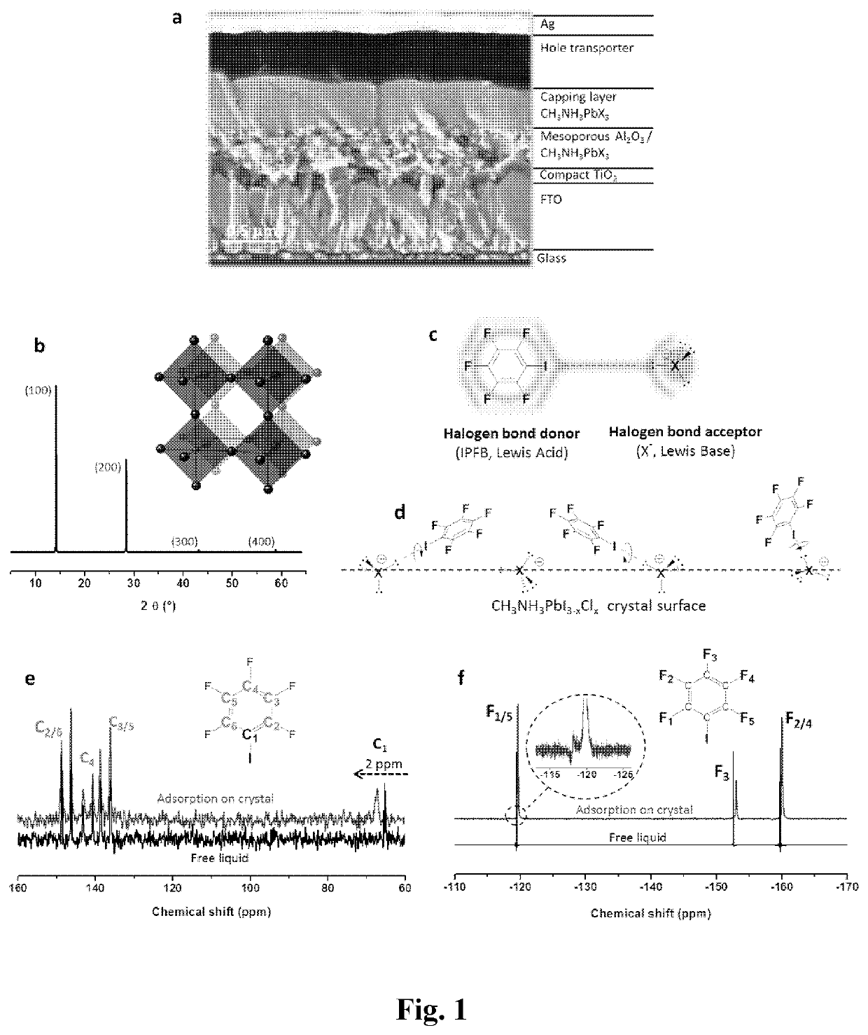
[0349]To demonstrate the presence of adsorbed IPBF (iodopentafluorobenzene) and the nature of the interaction with the CH3NH3PbX3 crystal surface (X=halide), solid state 13C and 19F nuclear magnetic resonance (NMR) measurements were performed. FIG. 1e shows the chemical shift of 13C NMR for pure IPFB, which is liquid at room temperature, and for IPFB adsorbed on the perovskite surface. No significant shift was found for the fluorine-bound carbons (C2-6) in the range 135-150 ppm, while the signal of the iodine-bearing carbon (C1) shifted 2 ppm downfield. Thus, 13C NMR gives strong evidence that IPFB is adsorbed via halogen bonding to the CH3NH3PbX3 crystal surface, as illustrated in FIG. 1d.

[0350]FIG. 1f shows 19F NMR collected on the same samples, which allows the extraction of more detailed information than 13C NMR. The 19F IPBF signals recorded on the treated perovskite films are made of two components (inset FIG. 1f), one small compone...

example 2

Passivation Procedure in Meso-Superstructured Solar Cells (MSSCs) with IPFB

[0351]The devices were prepared on patterned semi-transparent fluorine-doped tin oxide (FTO). A compact layer of 70 nm thick TiO2 was deposited via spray pyrolysis at 275° C. from a precursor solution of titanium diisopropoxide bis(acetylacetonate) diluted with anhydrous ethanol at a volume ratio of 1:10. The substrate was sintered at 500° C. for 45 min and left to cool to room temperature. The samples were then submerged in a 15 mM aqueous TiCl4 bath at 70° C. for 1 h, followed by rinsing with deionized water and re-sintering at 500° C. for 45 min. The next layer of mesoporous Al2O3 was deposited by spin coating a colloidal dispersion of Al2O3 nanoparticles in isopropanol (Sigma-Aldrich) diluted with isopropanol at a volume ratio of 1:2, at 2000 rpm (ramp: 2000 rpm / s) for 60 s, followed by drying at 150° C. for 30 min. The perovskite precursor (40 wt % of methylammonium iodide (CH3NH3I) and lead (II) chlorid...

example 3

Performance and Optical Properties of MSSCs with IPFB

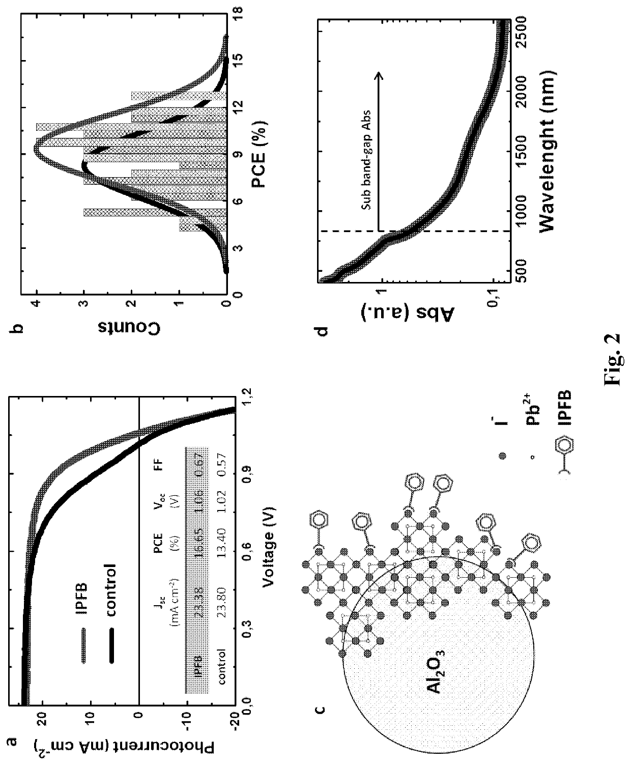
[0353]JV characteristics of the best perovskite MSSCs with and without IPFB treatment (produced by the above described method) are shown in FIG. 2a. Upon IPFB treatment, the short-circuit current density (Jsc) as well as the open-circuit voltage (Voc) remain similar, while the fill factor (FF) is dramatically improved. The table inset in FIG. 2b shows that the overall PCE (power conversion efficiency) increases from 13% to over 16%, representing a step improvement. In FIG. 2b the PCE statistical distribution for a set of devices prepared simultaneously is shown, which confirms the improved trend.

[0354]In FIG. 2a, the control device exhibits a slight bend in the JV curve near 0.9 V, which is responsible for the relatively poor fill factor. Similarly shaped JV curves have previously been reported in several works for both organic and inorganic solar cells, and it is been generally referred to as an “S-shaped” JV curve (Kumar, A. et ...


PUM


Abstract

The present invention relates to devices comprising metal halide perovskites and organic passivating agents. In particular, the invention relates to photovoltaic and optoelectronic devices comprising passivated metal halide perovskites. The device according to the invention comprises: (a) a metal halide perovskite; and (b) a passivating agent which is an organic compound; wherein molecules of the passivating agent are chemically bonded to anions or cations in the metal halide perovskite. The invention also provides a process for producing a photovoltaic device, which photovoltaic device comprises: (a) a metal halide perovskite; and (b) a passivating agent which is an organic compound; wherein molecules of the passivating agent are chemically bonded to anions or cations in the metal halide perovskite, wherein the process comprises treating a metal halide perovskite with a passivating agent, which passivating agent is an organic compound and is suitable for chemically bonding to anions or cations in the metal halide perovskite.

Description

CROSS-REFERENCE TO RELATED APPLICATIONS[0001]This application represents the national stage entry of PCT International Application No, PCT / GB2014 / 053735 filed Dec. 17, 2014 and claims priority to Great Britain Patent Application No. 1322310.2 filed Dec. 17, 2013 and Great Britain Patent Application No. 14138556 filed Aug. 5, 2014. The contents of these applications are hereby incorporated by reference as if set forth in their entirety herein.FIELD OF THE INVENTION[0002]The present invention relates to devices comprising metal halide perovskites and organic passivating agents. In particular, the invention relates to photovoltaic and optoelectronic devices comprising passivated metal halide perovskites.BACKGROUND OF THE INVENTION[0003]Photovoltaic (PV) cells, capable of converting sunlight directly into electricity, could ultimately be the solution to global energy demand. When the first crystalline silicon (c-Si) PV device was demonstrated in 1954, the envisaged manufacturing costs m...

Claims


Application Information

Patent Timeline
Patent Type & Authority Patents(United States)
IPC IPC(8): H01L31/0216H01L51/00H01L51/44H01L31/032H01L31/077H01L31/18H01L51/42
CPCH01L31/077H01L51/448H01L51/0032H01L31/1868H01L31/032H01L31/02167Y02P70/50H01L51/4213H01L2251/306Y02E10/549H01L51/4226Y02E10/547H10K85/00H10K30/151H10K30/10H10K2102/102H10K85/50H10K30/88
Inventor SNAITH, HENRY J.ABATE, ANTONIONOEL, NAKITA K.
Owner OXFORD UNIV INNOVATION LTD
Why Eureka
Try Eureka