

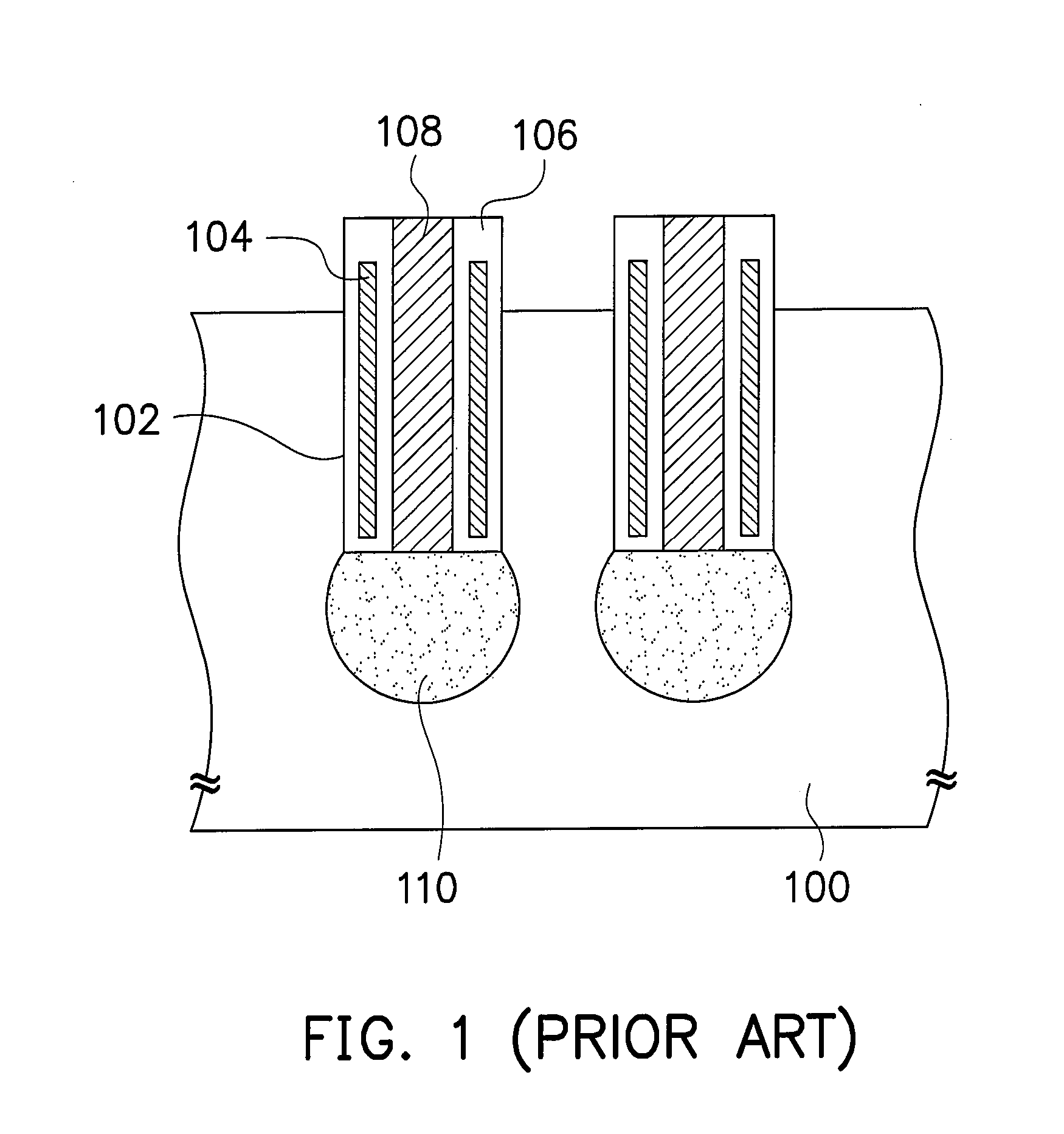
Manufacturing method of Anti-punch-through semiconductor device
a manufacturing method and semiconductor technology, applied in the field of semiconductor devices, can solve the problems of abnormal electric punching in the adjacent source/drain region, low operation speed, and high integration of device processing, and achieve the effects of low operation speed, reduced yield, and low performance efficiency
- Summary
- Abstract
- Description
- Claims
- Application Information
AI Technical Summary
Benefits of technology
Problems solved by technology
Method used
Image

Examples
Embodiment Construction
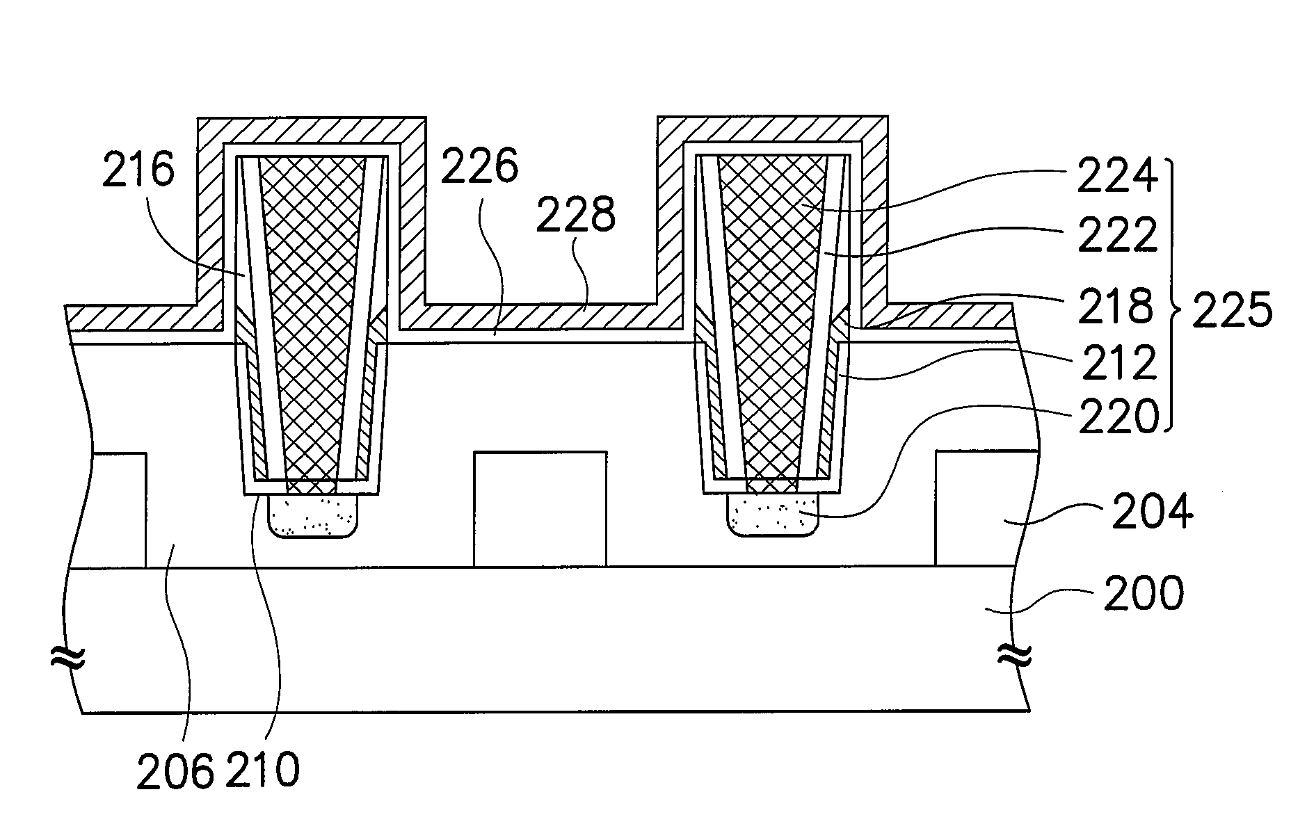
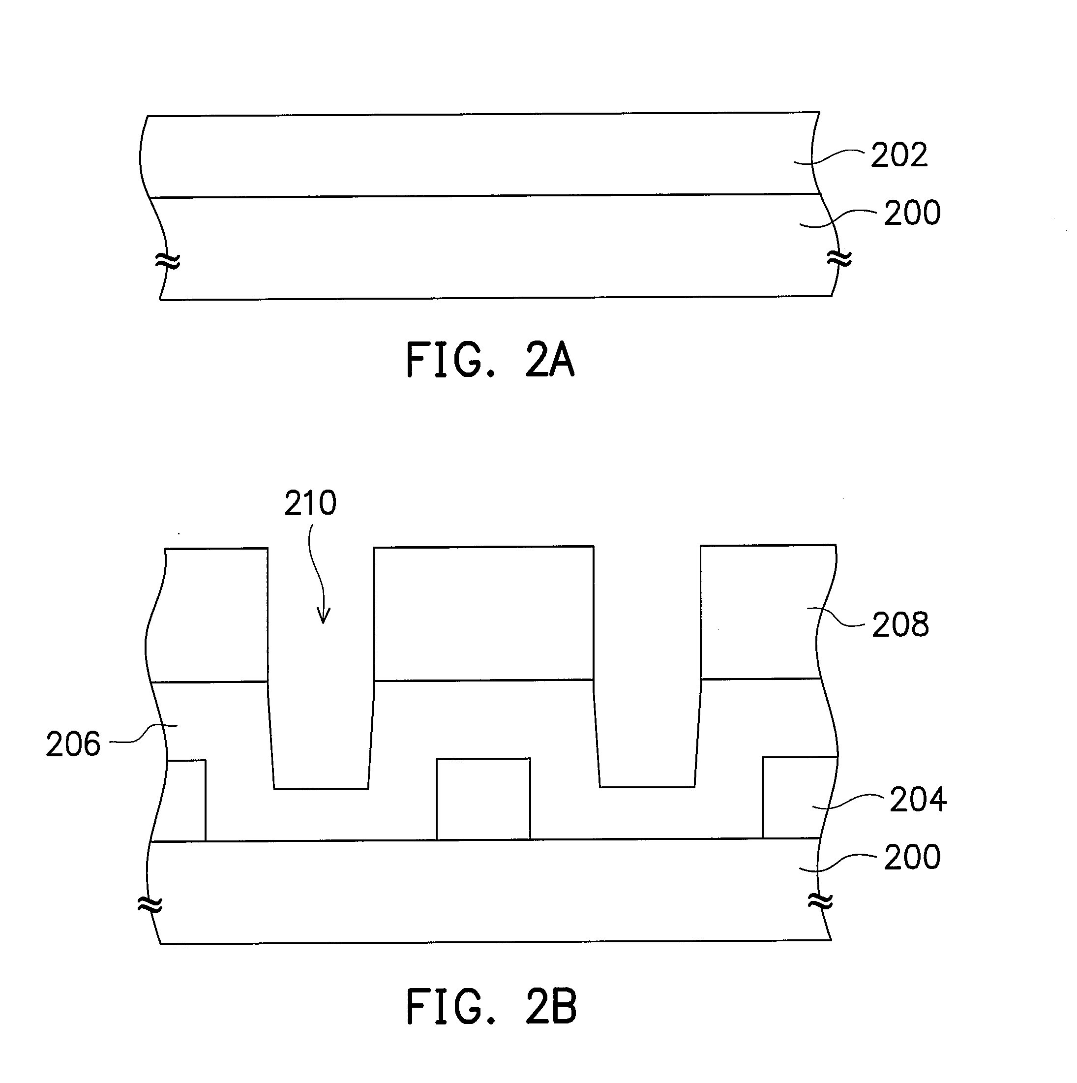
[0028]FIG. 2A to FIG. 2G are cross-sectional views showing the flowcharts of manufacturing the anti-punch-through semiconductor device according to the embodiment of the present invention. The trench memory is described in the following as an example.
[0029]First, referring to FIG. 2A, a substrate 200 is provided, and the substrate 200 is, for example, a silicon substrate. Next, an insulation layer 202 is formed on the substrate 200. Wherein, the material of the insulation layer is, for example, silicon oxide, and the thickness of the insulation layer 202 is about 100 Å-1000 Å, and the forming method is, for example, a chemical vapor deposition process.
[0030]Next, referring to FIG. 2B, the insulation layer 202 is patterned by photolithography process and etching process, and an isolation region 204 is formed on the substrate 200. Note that the isolation region is different from the shallow trench isolation structure used to form the active region. The isolation region of the present ...
PUM
 Abstract
Description
Claims
Application Information