Method for producing printed wiring board and protective film

A technology for a printed wiring board and a manufacturing method, which is applied in the manufacturing of printed circuits, printed circuits, and multilayer circuits, etc., can solve the problems of large difference in thermal expansion coefficient, inability to fully ensure temperature cycle reliability, and large thermal expansion coefficient.

Inactive Publication Date: 2018-10-16
NIPPON MEKTRON LTD
View PDF8 Cites 0 Cited by
  • Summary
  • Abstract
  • Description
  • Claims
  • Application Information

AI Technical Summary

Problems solved by technology

However, in liquid crystal polymers, the thermal expansion coefficient in the thickness direction is larger than that of conventional insulating materials such as polyimide, and the difference in thermal expansion coefficient between plated through holes, which are generally used as interlayer connection paths, is large.
Therefore, in the case of making the insulating base base material containing the liquid crystal polymer thick, there is a danger that the reliability against temperature cycles and the like cannot be sufficiently ensured.

Method used


Image

  • Method for producing printed wiring board and protective film
  • Method for producing printed wiring board and protective film
  • Method for producing printed wiring board and protective film

Examples


no. 1 approach

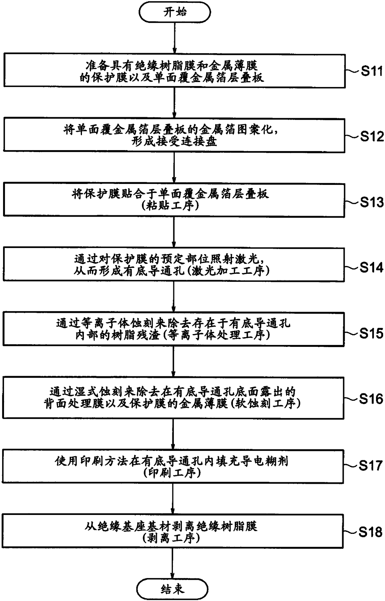
[0101] In the method of manufacturing a printed wiring board according to the first embodiment of the present invention, along figure 1 The flow chart is described. In this embodiment, a single-sided metal foil-clad laminate is used as a starting material.

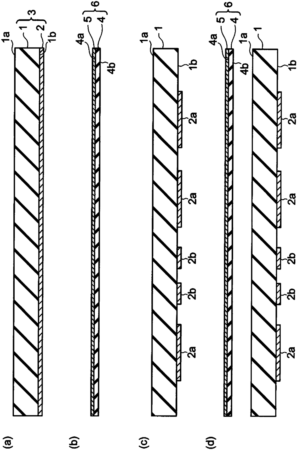
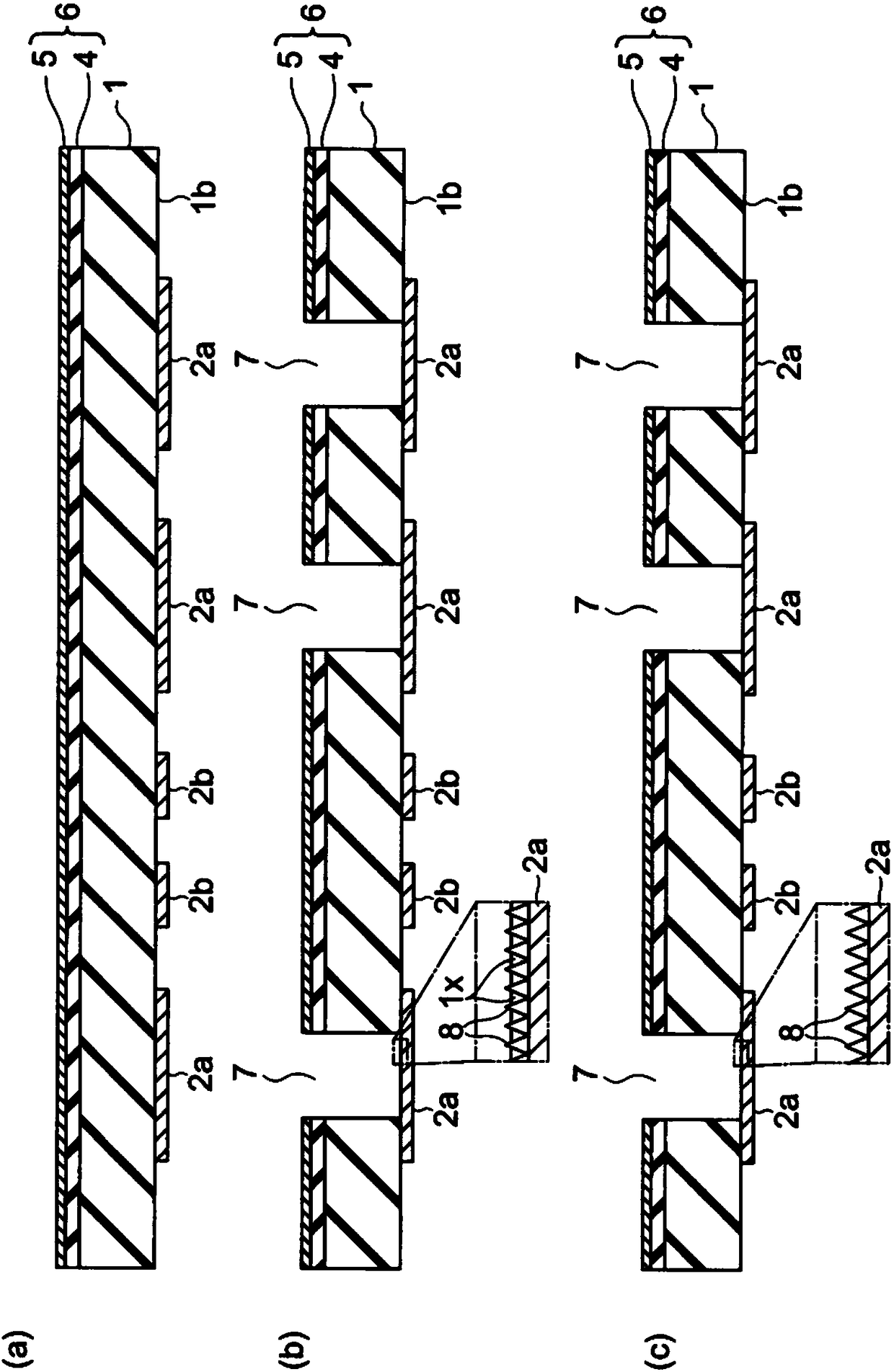
[0102] First, the single-sided metal foil-clad laminate 3 and the protective film 6 are prepared (step S11). Such as figure 2 As shown in (a), the single-sided metal foil-clad laminate 3 has an insulating base material 1 and a metal foil 2 (first metal foil) formed on one side of the insulating base material 1 . The insulating base material 1 has a main surface 1a (first main surface) and a main surface 1b (second main surface) opposite to the main surface 1a. In this embodiment, the main surface 1 a is the upper surface of the insulating base material 1 , and the main surface 1 b is the lower surface of the insulating base material 1 .

[0103] The insulating base material 1 is, for example, an insulating film forme...

no. 2 approach

[0141]In the method of manufacturing a printed wiring board according to the second embodiment of the present invention, along Image 6 The flow chart is described. In this embodiment, a double-sided metal foil-clad laminate is used as a starting material.

[0142] First, the double-sided metal foil-clad laminate 24 and the protective film 6 are prepared (step S21). Such as Figure 7 As shown in (a), the double-sided metal foil-clad laminate 24 has an insulating base material 21, a metal foil 22 (first metal foil), and a metal foil 23 (second metal foil). The insulating base material 21 has a main surface 21a (first main surface) and a main surface 21b (second main surface) opposite to the main surface 21a. In this embodiment, the main surface 21 a is the upper surface of the insulating base material 21 , and the main surface 21 b is the lower surface of the insulating base material 21 .

[0143] The insulating base material 21 is, for example, an insulating film formed of...

no. 3 approach

[0162] In the method of manufacturing a printed wiring board according to the third embodiment of the present invention, along Figure 10 The flow chart is described. In this embodiment, a multilayer printed wiring board is produced using the wiring base material 10 produced in the first embodiment and the wiring base material 30 produced in the second embodiment as starting materials.

[0163] First, the wiring base material 10 and the wiring base material 30 are prepared (step S31). Such as Figure 4 As shown, the wiring base material 10 has the protrusion part 9a obtained in the peeling process (process S18 of 1st Embodiment). Such as Figure 9 As shown, the wiring base material 30 has the protrusion part 27a obtained in the peeling process (process S29 of 2nd Embodiment).

[0164] Next, if Figure 11 As shown, the wiring base material 10 and the wiring base material 30 are aligned and stacked so that the protruding portion 9a and the protruding portion 27a are in cont...


PUM


Abstract

The present invention provides a method for producing a printed wiring board and a protective film. The method is capable of preventing a decrease in etching efficiency and protecting an insulating resin film adhered to a metal foil-clad laminate in a plasma treatment step of removing a resin residue. The method for producing the printed wiring board according to the present invention includes a step of preparing a single-sided metal foil-clad laminate having an insulating base substrate and a metal foil, and a protective film having an insulating resin film and a metal thin film; a step of bonding the protective film to the single-sided metal foil-clad laminate; a step of irradiating a predetermined portion of the protective film with a laser to form a bottom via; a step of removing the resin residue by plasma etching; a step of removing a back processing film and the metal thin film of a bottom surface of the bottom via by wet etching; a step of filling the conductive paste in the bottom via by a printing method; and a step of peeling off the insulating resin film from the insulating base substrate.

Description

technical field [0001] The present invention relates to a method for manufacturing a printed wiring board and a protective film, and more specifically, to a method for manufacturing a printed wiring board in which interlayer connections are made with a conductive paste, and to a method for use in the method for manufacturing the printed wiring board. protective film. Background technique [0002] Along with progress in miniaturization and higher functionality of electronic equipment, there is an increasing demand for higher densification of printed wiring boards. To meet this demand, multilayer printed wiring boards have been developed. In addition, Patent Document 1 describes a hybrid multilayer circuit board as a step in increasing the density. This hybrid multilayer circuit board has two multilayer circuit boards (rigid circuit boards) and a flexible printed wiring board (or flexible flat cable) that connects these multilayer circuit boards. These distribution boards a...

Claims


Application Information

Patent Timeline
Patent Type & Authority Applications(China)
IPC IPC(8): H05K3/46
CPCH05K3/4611H05K3/4688H05K2203/095H05K2203/107
Inventor 松田文彦成泽嘉彦
Owner NIPPON MEKTRON LTD
Why Eureka
Try Eureka