
Anti-punch-through semiconductor device

a technology of anti-punch-through and semiconductor devices, which is applied in the direction of semiconductor devices, electrical apparatus, transistors, etc., can solve the problems of abnormal electric punch-through in the adjacent source/drain region, low operation speed, and high device integration speed, so as to reduce yield, low operation speed, and low performance efficiency

Active Publication Date: 2008-10-28
POWERCHIP SEMICON MFG CORP
View PDF2 Cites 2 Cited by
  • Summary
  • Abstract
  • Description
  • Claims
  • Application Information

AI Technical Summary

Benefits of technology

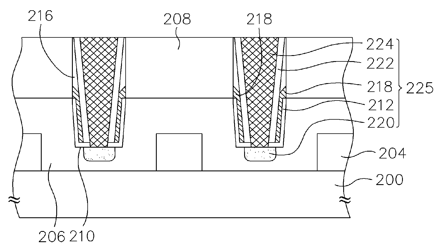
[0009]Another objective of the present invention is to provide an anti-punch-through semiconductor device, wherein, the isolation region between the source / gate regions can avoid the electric punch-through between the devices.
[0022]In the present invention, an isolation region is formed between two adjacent trench devices, so as to avoid adjacent source / drain regions during the ion-implanting process of forming the doped polysilicon from the electric punch-though as the dopant diffuses into the source / drain region to extend the region. And, the problem of the low operation speed and low performance efficiency due to the electric punch-through and reduced yield and reliability of the whole process, can also be avoided.

Problems solved by technology

When the distance reduces to some degree, the process problem due to the high integration of device may occur.
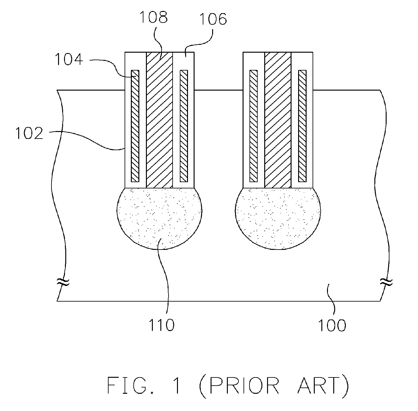
However, along with increased integration, in the process of forming the gate made of doped polysilicon, the dopant may diffuse into the source / drain region 110 to extend the region, which may easily cause the abnormal electric punch-through in the adjacent source / drain regions 110.
The problem of the electric punch-through may cause abnormal electric connection between adjacent trench devices, which may result in low operation speed and low performance efficiency, and even short or open circuit of the devices.
Accordingly, the yield and reliability of the whole process are adversely affected.

Method used


Image

  • Anti-punch-through semiconductor device
  • Anti-punch-through semiconductor device
  • Anti-punch-through semiconductor device

Examples


Embodiment Construction

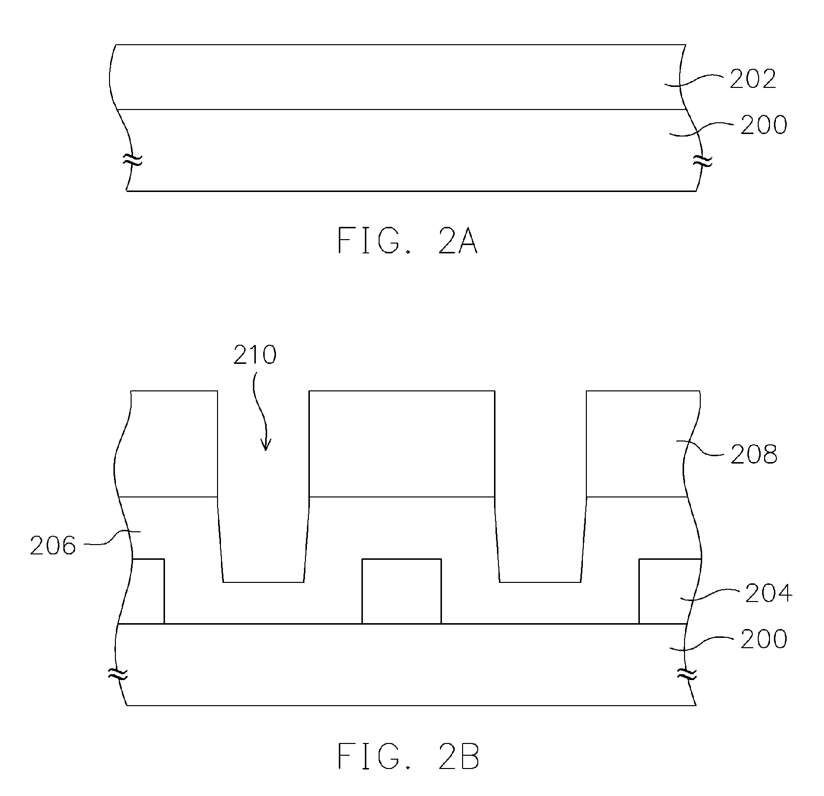
[0028]FIG. 2A to FIG. 2G are cross-sectional views showing the flowcharts of manufacturing the anti-punch-through semiconductor device according to the embodiment of the present invention. The trench memory is described in the following as an example.

[0029]First, referring to FIG. 2A, a substrate 200 is provided, and the substrate 200 is, for example, a silicon substrate. Next, an insulation layer 202 is formed on the substrate 200. Wherein, the material of the insulation layer is, for example, silicon oxide, and the thickness of the insulation layer 202 is about 1000 Å-10000 Å, and the forming method is, for example, a chemical vapor deposition process.

[0030]Next, referring to FIG. 2B, the insulation layer 202 is patterned by photolithography process and etching process, and an isolation region 204 is formed on the substrate 200. Note that the isolation region is different from the shallow trench isolation structure used to form the active region. The isolation region of the presen...


PUM


Abstract

An anti-punch-through semiconductor device is provided. The anti-punch-through semiconductor device includes a substrate, at least an isolation region and a plurality of trench devices. The trench device is disposed in the substrate. The trench device includes a source / drain region. The source / drain region of the trench device is disposed at the bottom of the trench device. The isolation region is disposed in the substrate and between the source / drain regions of each trench device.

Description

CROSS-REFERENCE TO RELATED APPLICATION[0001]This application claims the priority benefit of Taiwan application serial no. 94122056, filed on Jun. 30, 2005. All disclosure of the Taiwan application is incorporated herein by reference.BACKGROUND OF THE INVENTION[0002]1. Field of Invention[0003]The present invention relates to a semiconductor device and a manufacturing method thereof. More particularly, the present invention relates to an anti-punch-through semiconductor device and a manufacturing method thereof.[0004]2. Description of Related Art[0005]Along with the rapid development of the integrated circuit industry and the trend of high integration, the size of the entire circuit device is forced to be minimized to meet the requirement. When the size of the semiconductor reduces gradually, the distance between devices also relatively reduces. When the distance reduces to some degree, the process problem due to the high integration of device may occur. Therefore, it is a common obje...

Claims


Application Information

Patent Timeline
Patent Type & Authority Patents(United States)
IPC IPC(8): H01L29/76
CPCH01L27/115H01L27/11521H10B69/00H10B41/30
Inventor LAI, LIANG-CHUANWANG, PIN-YAO
Owner POWERCHIP SEMICON MFG CORP
Learn More