Electronic component and method of producing same

a technology of electronic components and production methods, applied in the field of electronic components, can solve the problems of troublesome handling of small-size base members, inability to ensure the prevention of short circuiting in subsequent steps, and difficulty in handling small-size base members, so as to ensure the prevention of short circuiting during production, reduce the number of scribing processes, and reduce production costs

Inactive Publication Date: 2008-09-11
CANON KK
View PDF11 Cites 5 Cited by
  • Summary
  • Abstract
  • Description
  • Claims
  • Application Information

AI Technical Summary

Benefits of technology

[0013]It is, therefore, an object of the present invention to provide a method of producing an electronic component and an electronic component in which the number of scribing processes is small and the productivity is high while short circuiting during production is surely prevented.
[0019]According to the present invention having the above-mentioned constitution, at least one of the following effects can be realized.1) An isolation region located among a plurality of electronic component portions provided on a large-size base member can be narrowed. As a result, it is possible to provide a plurality of large-size electronic component portions or a large number of electronic component portions on a large-size base member.2) A step of cutting a large-size base member also serves as a short ring cutting step. As a result, generation of dust can be reduced.3) The number of scribing processes can be reduced while short circuiting is surely prevented. For example, when four electronic components are to be obtained from a large-size base member, the necessary number of scribing processes is not 10 but at least 3.

Problems solved by technology

However, when small-size base members are to be obtained from the large-size base member, it is necessary to perform scribing at least ten times. Here, of the ten-time scribing, eight-time scribing must be accompanied by troublesome handling of the small-size base members.
Therefore, when the short ring is cut before the first two-time scribing, prevention of a short circuiting cannot be ensured in subsequent steps.
However, the handling of the small-size base members is complicated.

Method used


Image

  • Electronic component and method of producing same
  • Electronic component and method of producing same
  • Electronic component and method of producing same

Examples


first embodiment

[0028]An electronic component according to a first embodiment of the present invention is an electronic component comprising:

[0029]an electronic element disposed on a base member;

[0030]a take-out electrode connected to the electronic element; and

[0031]a short ring residue portion provided on a side of the base member without being connected to the electronic element.

[0032]To be more specific, the electronic component has the short ring residue portion which is not connected to the electronic element and provided on a side of the base member which is other than a side thereof on which the take-out electrode is disposed.

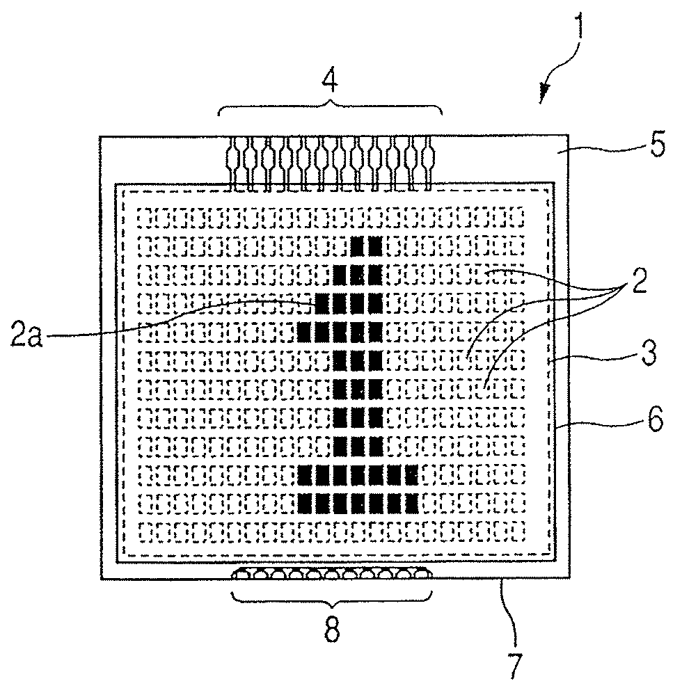
[0033]FIG. 1 is a schematic view showing an electronic component according to this embodiment. Examples of the electronic component include an electronic component having an organic EL element array. Reference numeral 1 denotes an electronic component, 2 denotes pixels, 2a denotes a displayed image, 3 denotes a display region, 4 denotes take-out electrodes, and 5 denot...

second embodiment

[0084]An electronic component according to this embodiment is an electronic component in which a short ring residue portion is disposed on a side intersecting with a side on which take-out electrodes are disposed. Other structures are identical to those of the electronic component according to the first embodiment.

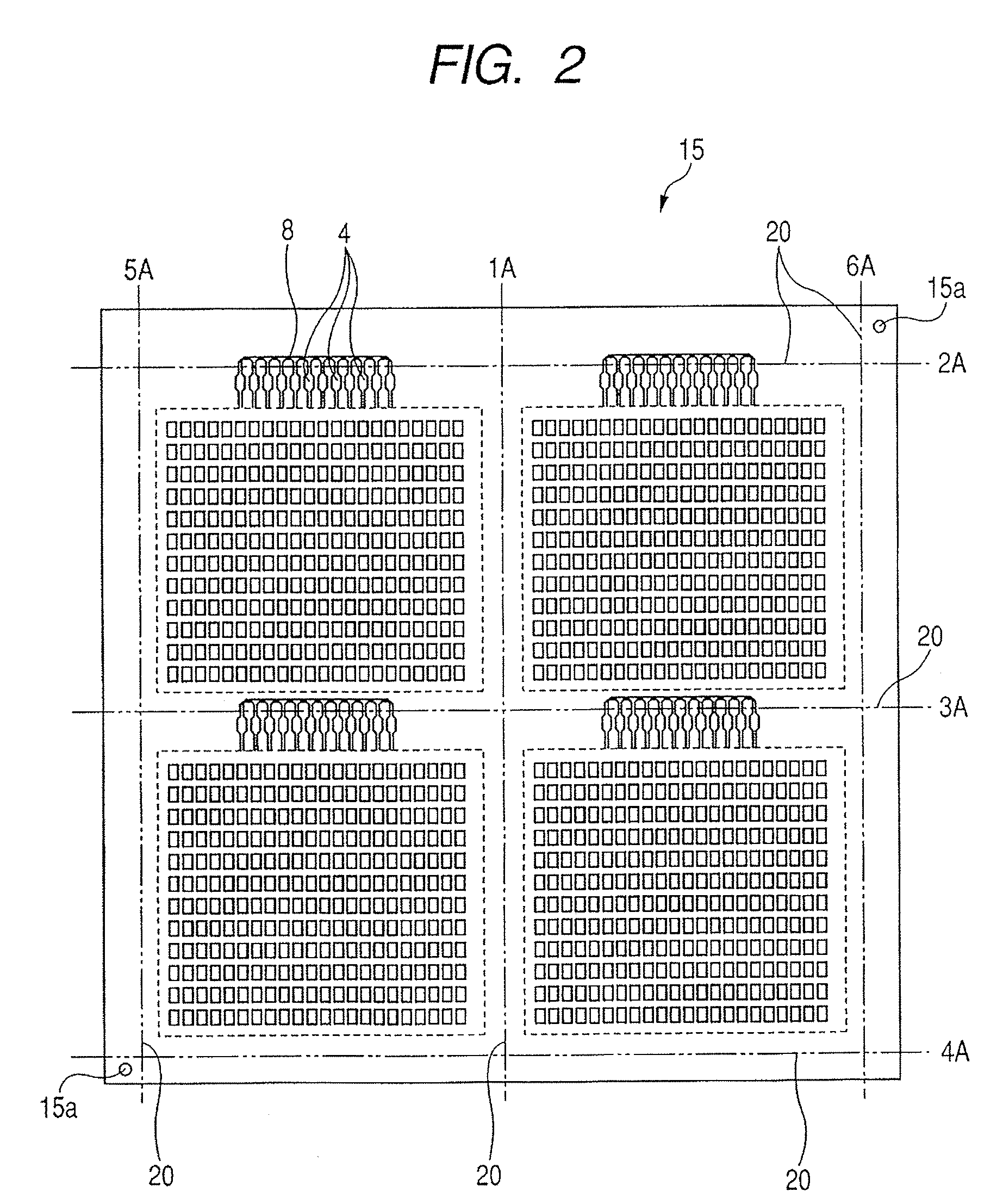
[0085]FIG. 5 is a schematic view showing the electronic component according to this embodiment. FIG. 5 shows four electronic components, each of which has the organic EL element array. Images of “1”, “2”, “3”, and “4” are displayed on display screens of the respective electronic components. Each of the electronic components on which the images “1” and “2” are displayed includes a short ring residue portion 8 disposed on a side of a base member which is other than a side thereof on which take-out electrodes 4 are disposed, of respective sides of the base member. To be more specific, the short ring residue portion 8 is disposed on a side located in a direction intersecting w...

third embodiment

[0088]An electronic component according to this embodiment is one of more than four electronic components obtained by cutting a large-size base member. Other structures are identical to those of the electronic component according to at least one of the first embodiment and the second embodiment.

[0089]FIG. 7 is a schematic view showing more than four electronic component portions disposed on a large-size base member before the electronic component according to this embodiment is obtained by cutting. FIG. 7 shows 25 electronic component portions.

[0090]As described above, the electronic component according to this embodiment is one of more than four electronic components obtained by cutting the large-size base member.

[0091]According to this embodiment, a large number of electronic components each having a small area can be disposed on a large-size base member having predetermined longitudinal and lateral dimensions.

[0092]Description is made by taking as an example a large-size base mem...


PUM


Abstract

There are provided an electronic component production method and an electronic component by which the number of scribing processes can be reduced and the productivity can be made higher while surely preventing short circuiting during the production. An electronic component including a short ring residue portion and a method of producing the electronic component are provided.

Description

BACKGROUND OF THE INVENTION[0001]1. Field of the Invention[0002]The present invention relates to an electronic component including an electronic element disposed on a base member (e.g., substrate) and a take-out electrode connected to the electronic element, and a method of producing the same.[0003]2. Related Background Art[0004]An electronic component including an electronic element and a take-out electrode is disclosed in Japanese Patent Application Laid-Open No. H07-181516 (JP 07-181516A).[0005]JP 07-181516A relates to a thin film transistor panel and describes transistors, gate lines connected to the transistors, and terminals thereof. The gate lines are connected to a conductive portion which is provided along side surfaces of a base member and then separated from the conductive portion by scribing. The thin film transistor panel is disposed on a large-size base member and respective liquid crystal display elements are obtained by scribing.[0006]JP 07-181516A describes that the...

Claims


Application Information

Patent Timeline
Patent Type & Authority Applications(United States)
IPC IPC(8): H01J9/26G09F9/00H01L21/301
CPCH01L25/046H01L27/1214H01L27/3276H01L2251/566H01L2924/0002H01L27/3293H01L2924/00H10K19/901H10K59/131H10K59/18H10K71/851G02F1/1345
Inventor NAKANE, NAOHIROTAKAHASHI, KIMIO
Owner CANON KK
Why Eureka
Try Eureka