Multilayered piezoelectric element and method of manufacturing the same
a piezoelectric element and multi-layer technology, applied in piezoelectric/electrostrictive transducers, device material selection, conductive pattern formation, etc., can solve the problems of difficult separation of the side electrode or the insulating electrode from the internal electrode, and improve the connection strength between the internal electrode and the side electrode or the insulating film, so as to improve the reliability of the operation the life of the piezoelectric element. , the effect o
- Summary
- Abstract
- Description
- Claims
- Application Information
AI Technical Summary
Benefits of technology
Problems solved by technology
Method used
Image
Examples
first embodiment
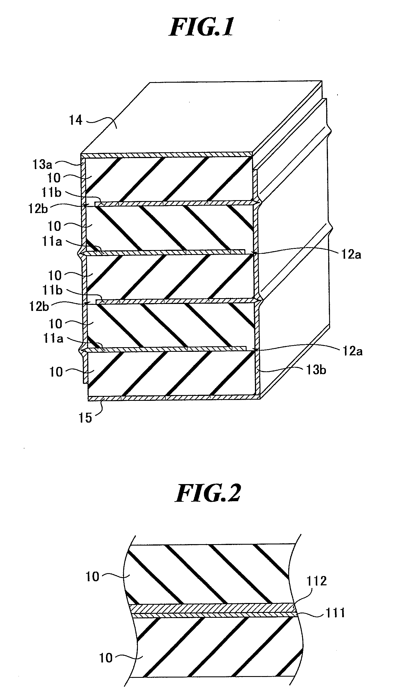
[0023]FIG. 1 is a partially sectional perspective view showing a structure of a multilayered piezoelectric element according to the present invention.
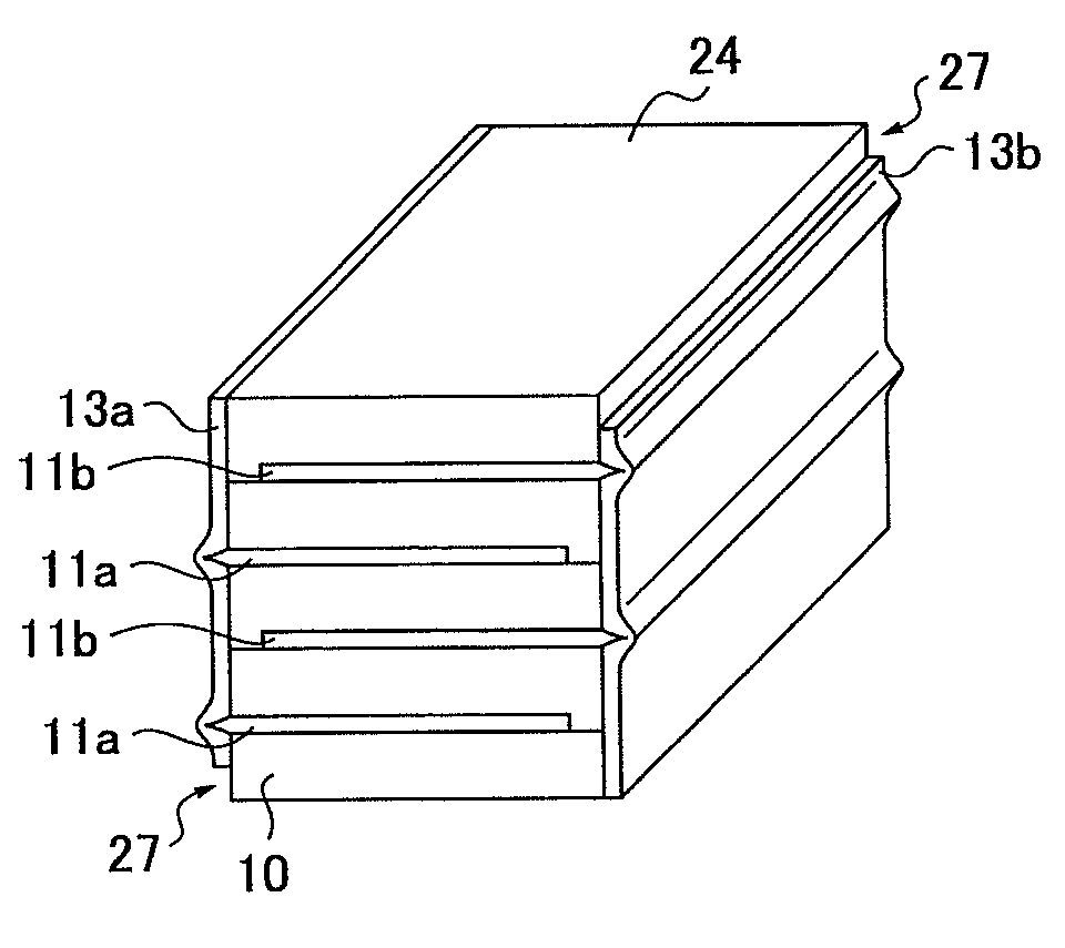
[0024]As shown in FIG. 1, the multilayered piezoelectric element according to the embodiment is a columnar structure having a bottom surface with sides of about 200 μm to 1 mm and a height of about 300 μm to 1 mm, for example. The multilayered piezoelectric element has (i) a multilayered structure including plural piezoelectric material layers 10, at least one internal electrode layer 11a and at least one internal electrode layer 11b, and (ii) side electrodes 13a and 13b formed on a first side surface and a second side surface of the multilayered structure, respectively. Generally, the multilayered piezoelectric element further has an upper electrode layer 14 and a lower electrode layer 15.
[0025]The at least one internal electrode layer 11a and at the least one internal electrode layer 11b are alternately stacked with the piezoelectric...
second embodiment
[0057]Next, a method of manufacturing the multilayered piezoelectric element according to the present invention will be explained by referring to FIGS. 6A-6D.
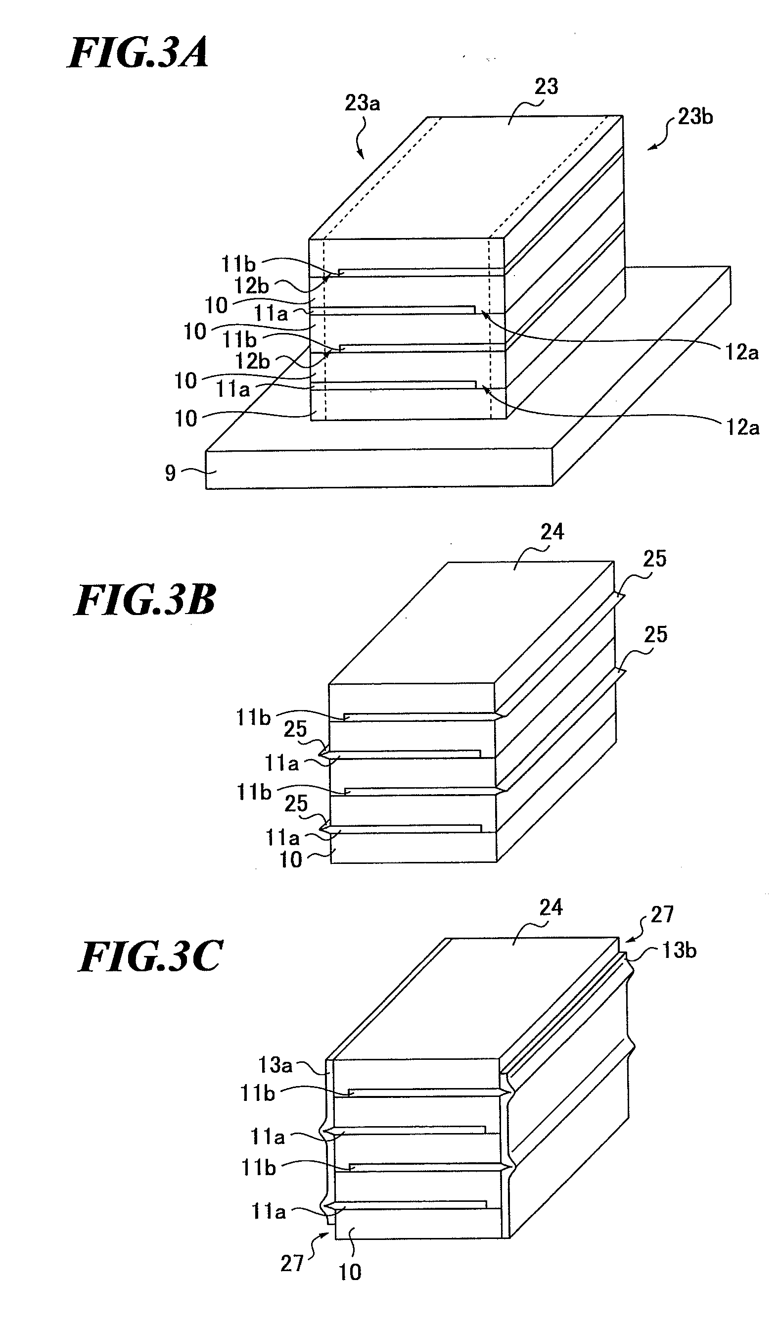
[0058]First, as shown in FIG. 6A, a multilayered structure 42 is formed by alternately stacking the piezoelectric material layers 30 and the internal electrode layers 31 on the substrate 9. The piezoelectric material layers 30 are formed by using the AD method as well as in the first embodiment. Further, the internal electrode layers 31 are formed by employing the same material as that explained in the first embodiment by sputtering or plating.
[0059]Then, the multilayered structure 42 is diced along dicing lines as shown in FIG. 6A. Thereby, as shown in FIG. 6B, a shaped multilayered structure 43 is obtained. End portions 44 of the internal electrode layers 31 protruding to the outer side than the piezoelectric material layers 30 are formed at the side surfaces of the diced multilayered structure 43. At this step, the substrate...
PUM
| Property | Measurement | Unit |
|---|---|---|
| height | aaaaa | aaaaa |
| height | aaaaa | aaaaa |
| thickness | aaaaa | aaaaa |
Abstract
Description
Claims
Application Information


