Electronic component, method for manufacturing electronic component, electronic apparatus, and moving object

a manufacturing method and electronic technology, applied in the field of electronic components, can solve the problems of heat generation of electronic components already mounted on circuit boards, complicated configuration of electronic components, and shrinkage of electronic components, so as to improve the reliability of bonding, reduce the size and thickness of electronic apparatuses, and improve the effect of bonding strength

Inactive Publication Date: 2016-01-28
SEIKO EPSON CORP
View PDF4 Cites 4 Cited by
  • Summary
  • Abstract
  • Description
  • Claims
  • Application Information

AI Technical Summary

Benefits of technology

[0027]According to this application example, the electronic component in which the possibility of weakening of the bonding strength between the connection pad and the connection terminal due to the cracking or explosive boiling of the electrically

Problems solved by technology

Recently, with reduction in the size and thickness of electronic apparatuses, the configuration of electronic components and the methods for mounting electronic components on wiring boards become more complicated and there are some cases where electronic components already mounted on a circuit board are subjected to heat.
If electronic components already mounted on a circuit board with an electrically conductive bonding member are subjected to heat in this manner, phenomena such as cracking due to expansion of air bubbles or the like contained in the electrically conductive bonding member or re-melting of the electrically conductive bonding member may occur, causing a risk that bonding failure such as an electrical conti

Method used


Image

  • Electronic component, method for manufacturing electronic component, electronic apparatus, and moving object
  • Electronic component, method for manufacturing electronic component, electronic apparatus, and moving object
  • Electronic component, method for manufacturing electronic component, electronic apparatus, and moving object

Examples


first embodiment

Configuration

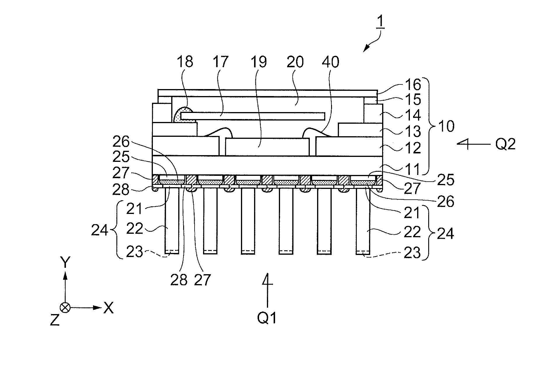
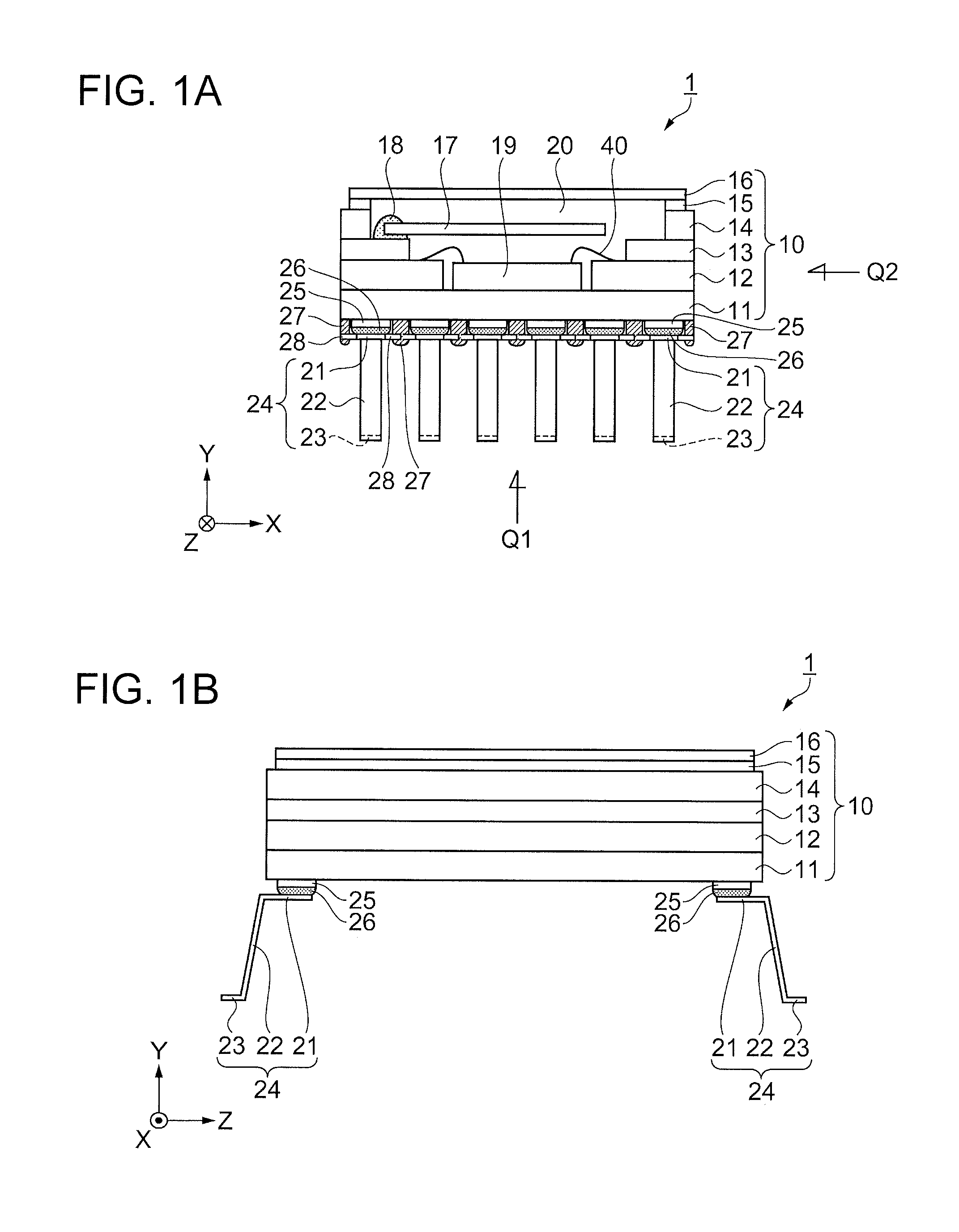
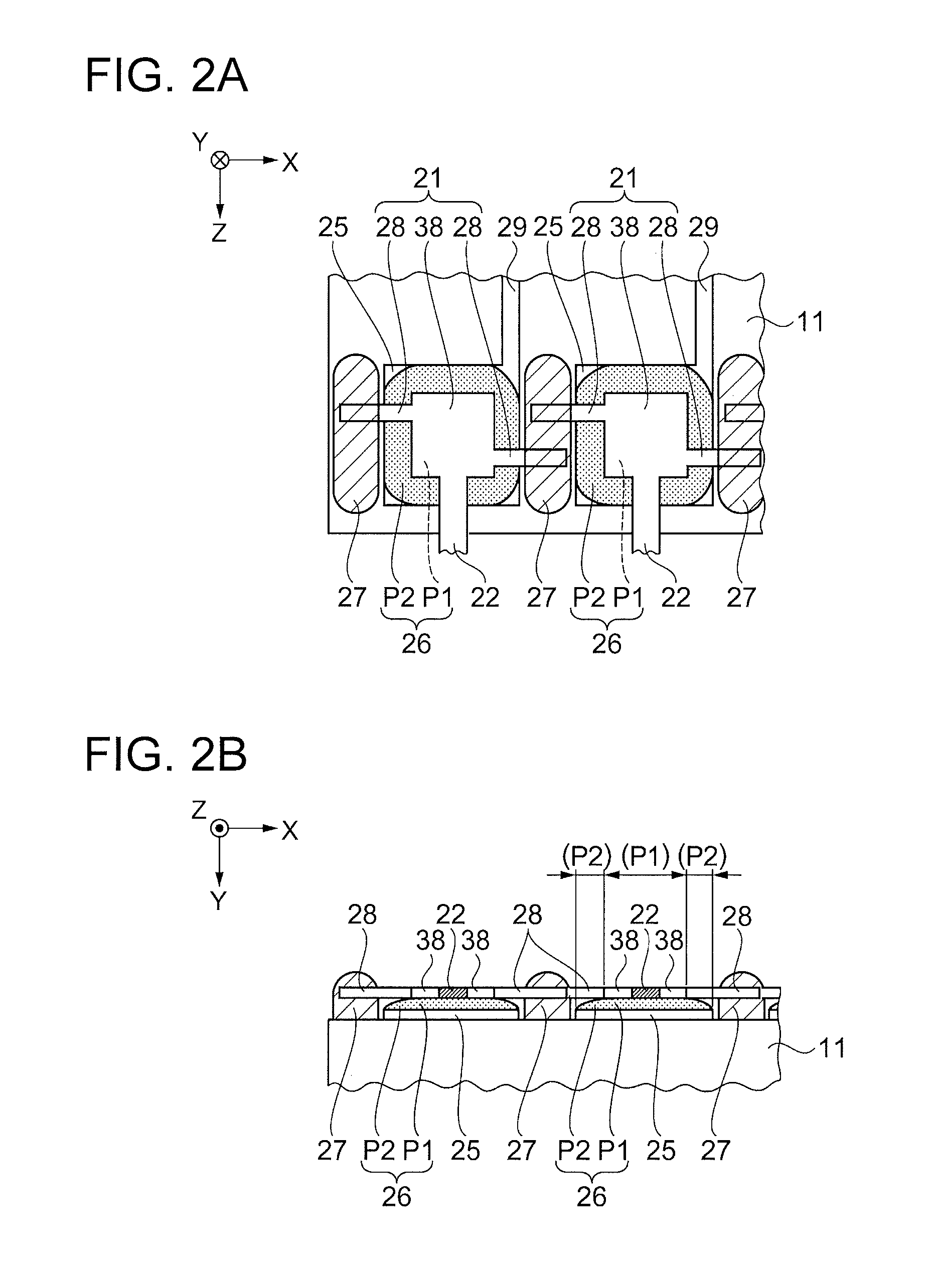
[0042]As an example of an oscillator according to a first embodiment of an electronic component according to the invention, a crystal oscillator having an SC-cut crystal oscillating piece with excellent frequency stability is employed and explained with reference to FIGS. 1A to 2B. FIGS. 1A and 1B are schematic views showing the structure of the oscillator according to the first embodiment of the electronic component according to the invention. FIG. 1A is a front cross-sectional view. FIG. 1B is a side view, as viewed in the direction of Q2 shown in FIG. 1A. FIGS. 2A and 2B show the schematic configuration of the connection site of the lead terminal of the oscillator according to the first embodiment. FIG. 2A is a bottom view, as viewed in the direction of Q1 shown in FIG. 1A. FIG. 2B is a front view of FIG. 2A. In the drawings including the drawings described below, X-axis, Y-axis and Z-axis are illustrated as three axes orthogonal to each other, as a matter of conveni...

second embodiment

[0072]As an example of an oscillator according to a second embodiment of the electronic component according to the invention, a crystal oscillator having an SC-cut crystal oscillating piece is employed and described with reference to FIGS. 4A and 4B.

[0073]FIGS. 4A and 4B are schematic views showing the structure of the oscillator according to the second embodiment of the electronic component according to the invention. FIG. 4A is a front cross-sectional view. FIG. 4B is a side view, as viewed in the direction of Q2 shown in FIG. 4A. The X-axis, Y-axis and Z-axis, and the top and bottom surface in the description are similar to those in the first embodiment.

[0074]The second embodiment has a configuration in which the direction of the container 10 with respect to the lead terminal 24 is different (vertically inverted) from that in the crystal oscillator 1 of the first embodiment. In this description, the different configuration from the first embodiment is mainly described and similar...

third embodiment

[0079]As an example of an oscillator according to a third embodiment of the electronic component according to the invention, a crystal oscillator having an SC-cut crystal oscillating piece is employed and described with reference to FIGS. 5A and 5B.

[0080]FIGS. 5A and 5B are schematic views showing the structure of the oscillator according to the third embodiment of the electronic component according to the invention. FIG. 5A is a front cross-sectional view. FIG. 5B is a side view, as viewed in the direction of Q2 shown in FIG. 5A. In the description of the third embodiment, similar configurations to those of the first embodiment are denoted by the same reference numbers and will not be described further in detail.

[0081]As shown in FIGS. 5A and 5B, a crystal oscillator 1b of the third embodiment has a configuration in which a circuit element 30 and circuit components (not shown) are connected to the bottom surface (surface where the connection terminal 25 is provided) of the containe...


PUM


Abstract

To provide an electronic component in which the bonding position and bonding strength of a lead terminal can be maintained even if re-heated, a crystal oscillator as an electronic component includes: a first substrate having a connection terminal; and a lead terminal having a connection pad connected to the connection terminal of the first substrate via an electrically conductive bonding member. The electrically conductive bonding member has a part overlapping with the connection terminal and the connection pad, and a part arranged on the outside of the connection pad, as viewed in a plan view. The connection pad is provided with a first area overlapping with the connection terminal and a second area extending from the first area. The second area is connected to the first substrate via an insulative bonding member.

Description

BACKGROUND[0001]1. Technical Field[0002]The present invention relates to an electronic component, a method for manufacturing an electronic component, an electronic apparatus, and a moving object.[0003]2. Related Art[0004]According to the related art, in order to mount electronic components forming an electronic apparatus onto a circuit board, a method in which an external connection terminal (lead terminal) is connected to a connection terminal on a circuit board, using an electrically conductive bonding member such as solder, for example, is known. Recently, with reduction in the size and thickness of electronic apparatuses, the configuration of electronic components and the methods for mounting electronic components on wiring boards become more complicated and there are some cases where electronic components already mounted on a circuit board are subjected to heat. If electronic components already mounted on a circuit board with an electrically conductive bonding member are subjec...

Claims


Application Information

Patent Timeline
IPC IPC(8): H05K1/11H03B5/32H05K3/40
CPCH05K1/111H05K3/40H03B5/32B81C1/00261H01L23/13H01L23/15H01L23/49811H01L2224/48225H01L2924/15153H01L2924/1517H01L2924/15311
Inventor KONDO, MANABU
Owner SEIKO EPSON CORP
Why Eureka
Try Eureka