Slotted guide structure

Inactive Publication Date: 2008-09-18
COMMISSARIAT A LENERGIE ATOMIQUE ET AUX ENERGIES ALTERNATIVES
View PDF10 Cites 4 Cited by
  • Summary
  • Abstract
  • Description
  • Claims
  • Application Information

AI Technical Summary

Benefits of technology

[0013]The invention proposes an alternative manufacturing method which makes it possible to avoid the difficult step of filling the slot.
[0023]The thickness of the silica layer SiO2 forming the etching barrier layer is preferably greater than 1 μm for the purpose of preventing interference with the circuit situated below.

Problems solved by technology

However, no attempt at filling has thus far been concluded, in so far as a low deposition (for example by PECVD) temperature does not allow the slot 3 to be filled.
In this case, there is not only a bubble associated with a filling defect, but a filling defect.

Method used


Image

  • Slotted guide structure
  • Slotted guide structure
  • Slotted guide structure

Examples


Embodiment Construction

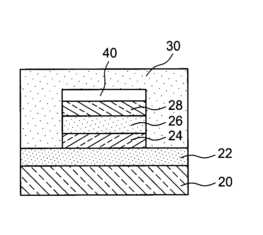
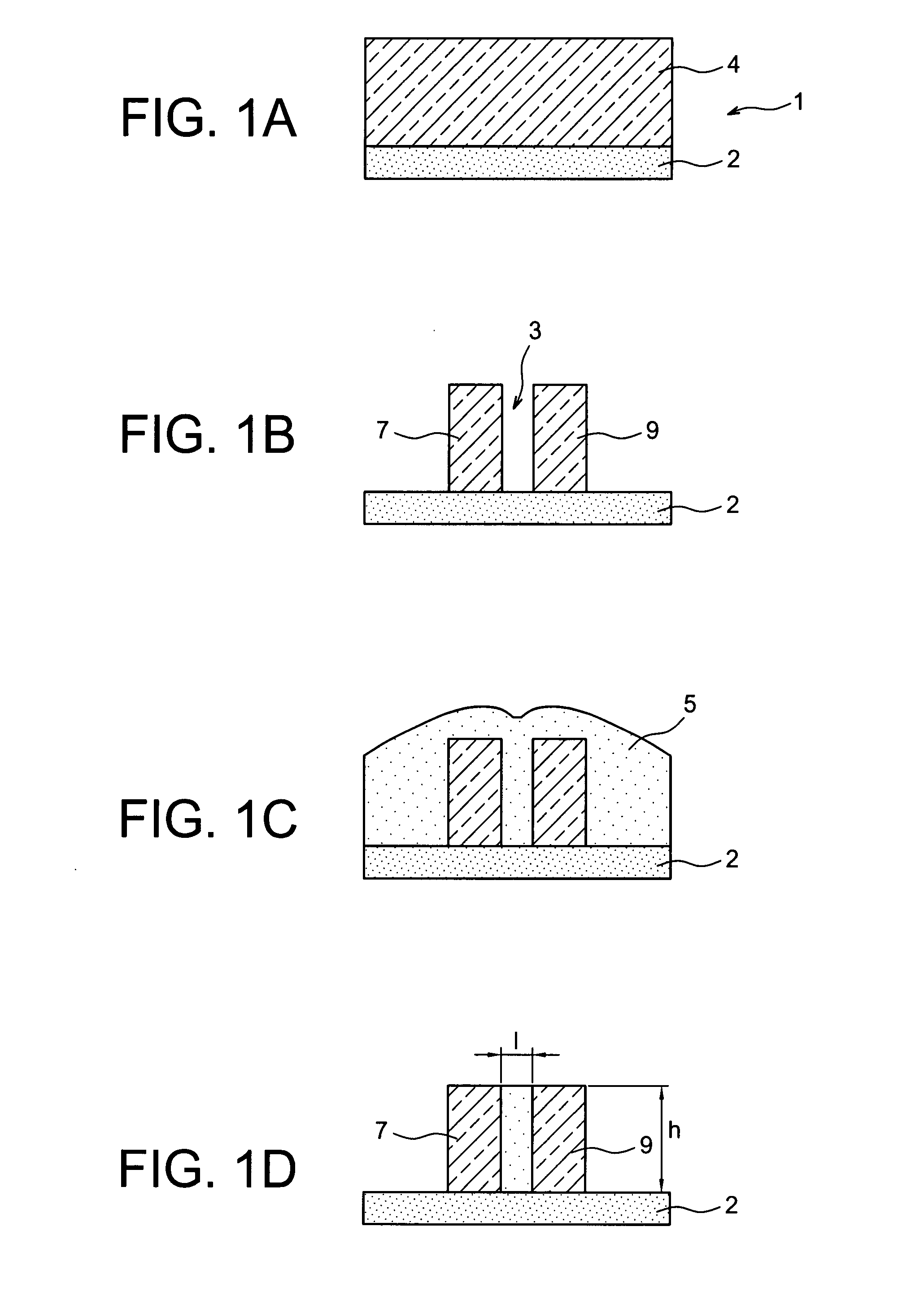
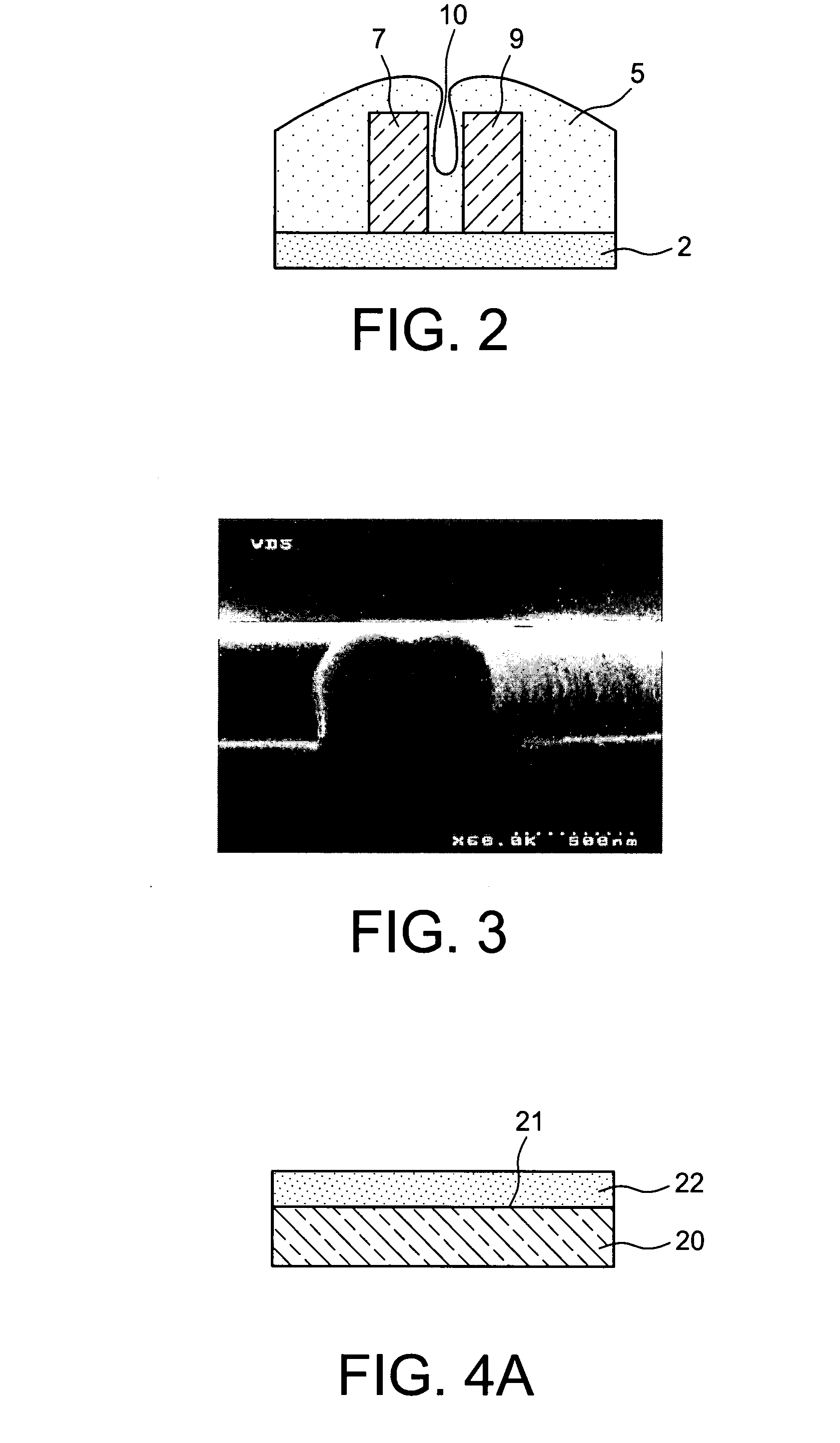
[0034]A first manufacturing method according to the invention will be described in connection with FIGS. 4A-4E.

[0035]In a first step, (FIG. 4A) the deposition or growth of a first oxide layer 22 (referred to as silica SiO2) is carried out on a planar surface 21 of a silicon substrate 20. The layer 22 of SiO2 can also be formed by oxygen implantation followed by annealing (SIMOX method).

[0036]A silicon layer 24 is then deposited or formed on the oxide layer 22. This layer 24, as well as the layers mentioned below, can be formed via PECVD or LPCVD.

[0037]According to the invention, it is thus possible to deposit the silicon 24 in amorphous form (PECVD deposition), using a standard silicon plate 20, having undergone a deposition 22 of silica or a thermal oxidation. The thickness of this oxide 22, preferably greater than 1 μm, is such that the losses induced by coupling with the substrate or with the CMOS circuit situated beneath the SiO2 are prevented.

[0038]A layer 26 of material having...


PUM


Abstract

The invention relates to a method for producing a slotted guide, in which:a) a layer of material having a refractive index less than that of silicon is formed on a first silicon layer which itself rests on a silica SiO2 layer, then:b) a second silicon layer is formed on the layer of material having a refractive index less than that of silicon, this second layer forming a stack with the layer of material having a refractive index less than that of silicon and the first silicon layer, the layer of material having a refractive index less than that of silicon being contained between said two silicon layers;c) this stack is etched, the silica layer SiO2 forming the barrier layer for this etching.

Description

CROSS-REFERENCE TO RELATED PATENT APPLICATION OR PRIORITY Claim[0001]This application claims the benefit of a French Patent Application No. 06-54670, filed on Oct. 31, 2006, the disclosure of which is incorporated herein in its entirety by reference.TECHNICAL FIELD AND PRIOR ART[0002]This invention is located in the field of “Silicon Nanophotonics” (the field of guiding light in guides of nanometric dimensions), and relates primarily to optical interconnections on silicon chips and in particular the production of photonic logic gates.[0003]Highly integrated optical functions can be produced on silicon. In a general approach, transmitters are used (integrated or added on, and electrically controlled), which are coupled with a set of guides which perform an optical function, either passively, or in response to an electrical command. These guides terminate at photodetectors which deliver the result of the optical function electrically.[0004]The operation of a slotted guide implements p...

Claims


Application Information

Patent Timeline
IPC IPC(8): B29D11/00
CPCB82Y20/00G02B6/136G02B6/1223
Inventor JORDANA, EMMANUELFEDELI, JEAN-MARCEL MELHAOUI, LOUBNA
Owner COMMISSARIAT A LENERGIE ATOMIQUE ET AUX ENERGIES ALTERNATIVES
Why Eureka
Try Eureka