Apparatus, unit and method for testing image sensor packages

a technology of image sensor and apparatus, applied in the direction of individual semiconductor device testing, material analysis, instruments, etc., can solve the problems of low productivity, high defective rate, and chip-on-board failures

Active Publication Date: 2008-09-18
OPTOPAC
View PDF15 Cites 15 Cited by
  • Summary
  • Abstract
  • Description
  • Claims
  • Application Information

AI Technical Summary

Benefits of technology

[0041]Preferably, a socket printed circuit board having top and bottom surfaces respectively formed with mutually connected upper and lower contact pads is attached to a bottom surface of the socket body, the socket body is formed with through-holes into which the connecting members are inserted so that lower ends of the connecting members are brought into contact with the upper contact pads, and the lower contact pads are brought into contact with contact members provided on the lower supporting

Problems solved by technology

Among several methods of directly mounting a bare chip of an image sensor on a camera module, a COB (Chip-On board) method which currently occupies 90% or more has problems such as low productivity caused by a unit level packaging scheme, a high defective rate caused by introduction of dust particles during fabrication processes, high investment and maintenance costs of equipment including a clean room having a high degree of cleanness, and limitations on miniaturization.
That is, all color filters and micro-lenses are very vulnerable to introduction of dust particles or penetration of moisture because they are fabricated through a photolithographic process after being coated with photoresist.
Generally, the most critical and frequent defect in a camera module is a defect of an image sensor, which is caused by a defect of an image sensor chip itself or introduction of dust into an image sensing area during a process of packing the image sensor chip.
That is, if dust particles are introduced into the image sensor package and then stick on the image sensing area, repeatable defects occur in photographed images.
Even though dust particles do not stick on the image sensing area, dust molecules moving in the image sensing area are not acceptable because they may cause defects in a non-repeatable manner.
It is known that in

Method used


Image

  • Apparatus, unit and method for testing image sensor packages
  • Apparatus, unit and method for testing image sensor packages
  • Apparatus, unit and method for testing image sensor packages

Examples


Embodiment Construction

[0052]Hereinafter, a preferred embodiment of the present invention will be described with reference with the accompanying drawings.

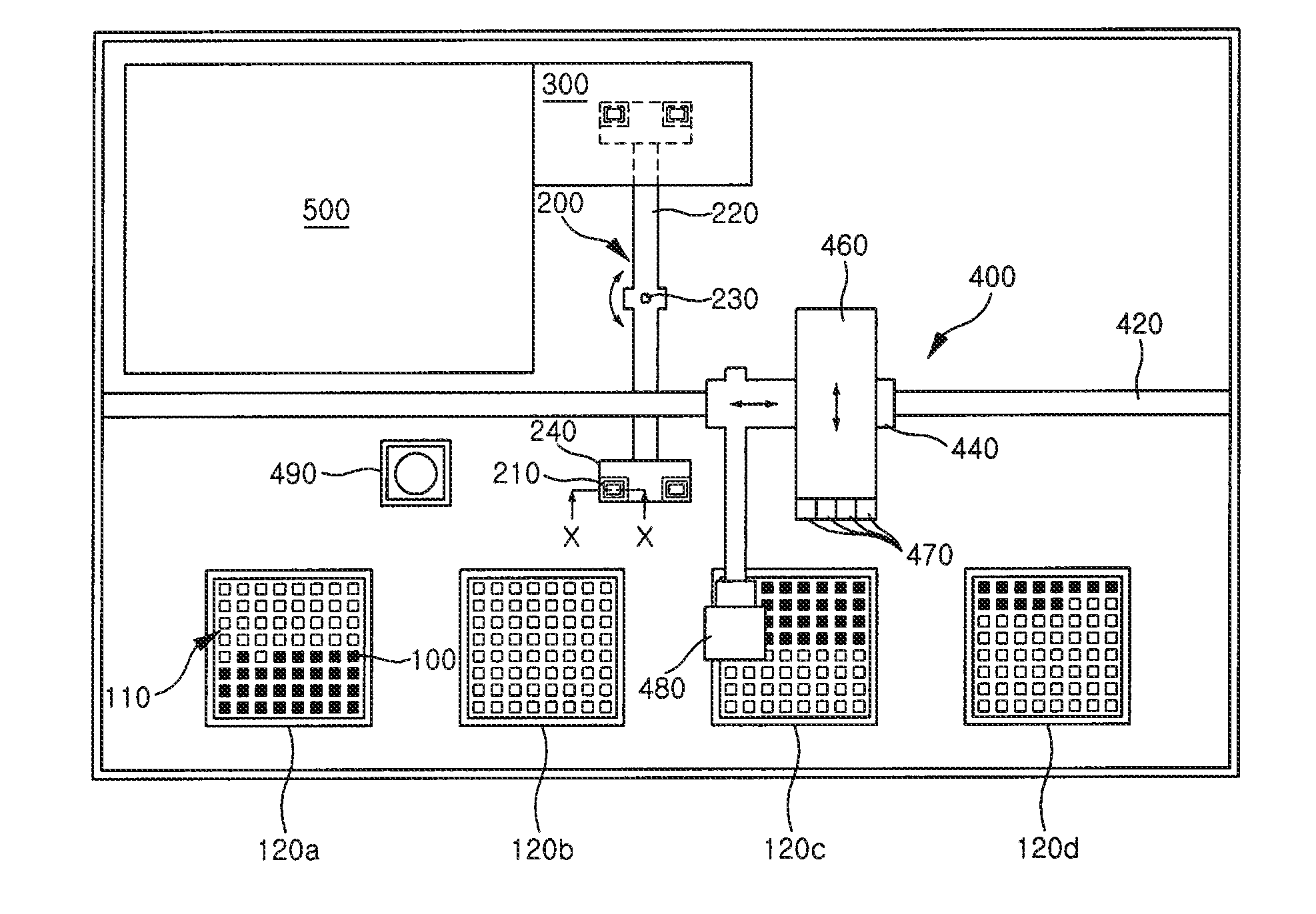
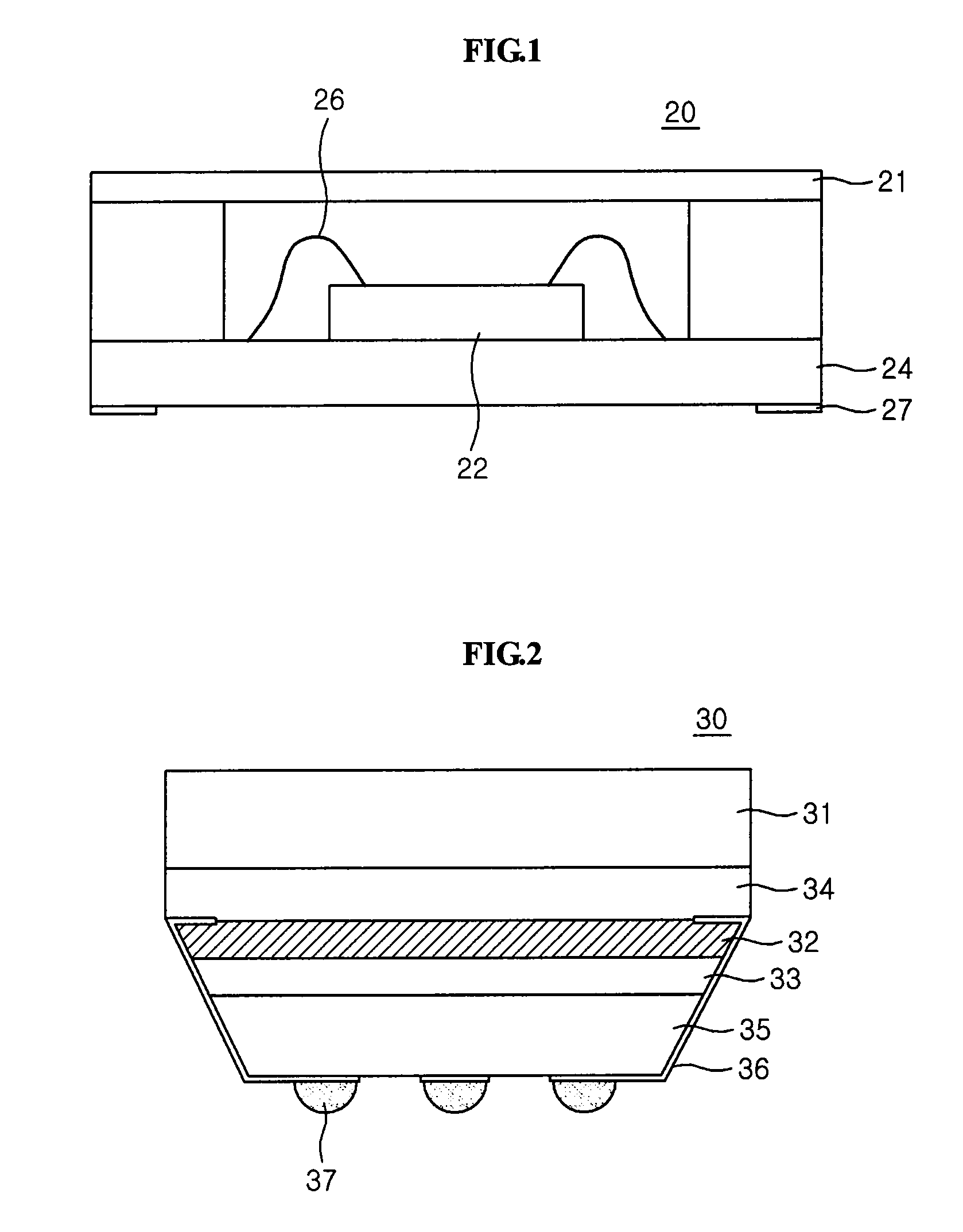
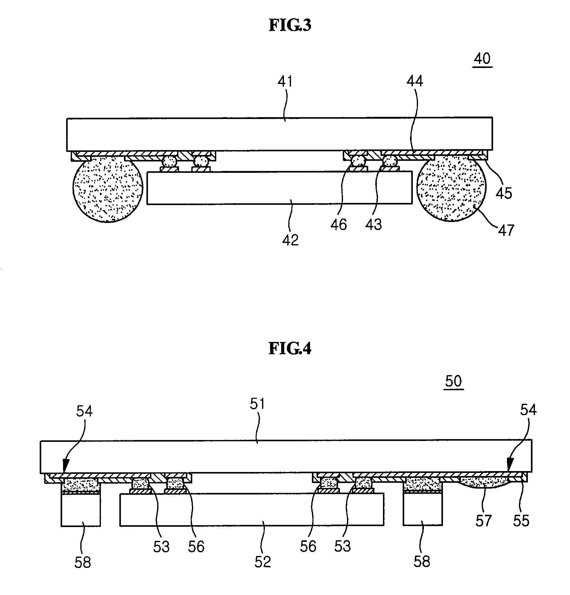
[0053]FIG. 5 is a plan view schematically showing the configuration of an apparatus for testing image sensor packages according to an embodiment of the present invention; FIG. 6 shows a tray for loading a plurality of image sensor packages on the apparatus for testing image sensor packages according to the present invention; FIG. 7 is a perspective view of a cassette with the tray loaded thereon; FIGS. 8A and 8B are enlarged sectional views taken along line X-X of FIG. 5, showing a socket base on which an image sensor package is to be seated; FIG. 9 is a sectional view of a pogo pin to be mounted on the socket base shown in FIGS. 8A and 8B; FIG. 10 is a perspective view showing that one of package picker units for carrying image sensor packages is mounted in front of a package picker mounting section; FIG. 11 is a sectional view of a testing section when...


PUM


Abstract

The present invention relates to an apparatus, unit and method for testing image sensor packages, which can automatically test whether the image sensor packages are defective before they are assembled into camera modules. An apparatus for testing image sensor packages according to the present invention comprises a seating unit on which image sensor packages are seated for tests; a testing section having a lens and a light source above the image sensor packages to perform an open and short test and an image test for the image sensor packages; and a controlling and processing unit having a tester module for performing the open and short test and the image test for the image sensor packages. A method for testing image sensor packages according to the present invention comprises the steps of connecting the image sensor packages to a tester module for performing tests for checking whether the image sensor packages are defective; and carrying out an open and short test and an image test for the image sensor packages while irradiating light on the image sensor packages through a lens or blocking the light.

Description

CROSS-REFERENCE TO RELATED APPLICATIONS[0001]This U.S. non-provisional patent application is a continuation of U.S. patent application Ser. No. 11 / 457,771, filed Jul. 14, 2006, and claims priority under 35 U.S.C. § 119 of Korean Patent Applications 2005-0121803 filed on Dec. 12, 2005 and 2005-0121805 filed Dec. 12, 2005, the entire contents of which are hereby incorporated by reference.FIELD OF THE INVENTION[0002]The present invention relates to an apparatus for testing photo-sensing semiconductor devices, and more particularly, to an apparatus, unit and method for testing image sensor packages, which can automatically test whether the image sensor packages are defective before they are assembled into camera modules.BACKGROUND OF THE INVENTION[0003]Image sensors are semiconductor devices having the function of photographing images of human beings or objects. The market of these image sensors has been rapidly expanded as they have been loaded into portable phones as well as common di...

Claims


Application Information

Patent Timeline
IPC IPC(8): G01R31/26
CPCH01L27/14618H01L2224/16H01L2924/1532H01L2924/15311H01L2924/01077H01L2224/05548H01L2224/05573H01L2224/05568H01L2224/056H01L2924/16195H01L2924/00014
Inventor KIM, YOUNG-SEOKLEE, HWAN-CHULJU, JAE-CHEOL
Owner OPTOPAC
Why Eureka
Try Eureka