Method for manufacturing display device

a display device and manufacturing method technology, applied in semiconductor devices, instruments, electrical devices, etc., can solve the problems of damage to the insulating layer stacking, reduce the number of photolithography steps, and reduce the cos

Inactive Publication Date: 2008-09-18
SEMICON ENERGY LAB CO LTD
View PDF17 Cites 47 Cited by
  • Summary
  • Abstract
  • Description
  • Claims
  • Application Information

AI Technical Summary

Benefits of technology

[0018]By the present invention, components such as a wiring included in a display device or the like and a contact hole for electrically connecting the components through an insulating layer can be formed with a reduced number of complicated photolithography steps. A display device can be manufactured through a simplified process. Therefore, there is not much loss of materials and the cost can be reduced. Accordingly, high performance and highly reliable display devices can be manufactured with a high yield.

Problems solved by technology

The light absorbing layer is heated by energy of the absorbed laser light and damages the insulating layer stacked thereover.

Method used


Image

  • Method for manufacturing display device
  • Method for manufacturing display device
  • Method for manufacturing display device

Examples


embodiment mode 1

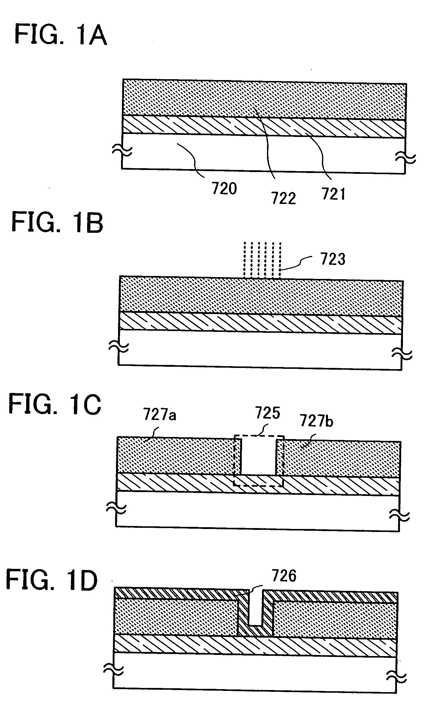
[0053]In this embodiment mode, a method for forming a contact hole through a highly reliable and more simplified process at low cost is described with reference to FIGS. 1A to 1D.

[0054]When thin films (for example, conductive layers or semiconductor layers) which are to be stacked with an insulating layer interposed therebetween are electrically connected, an opening (so-called contact hole) is formed in the insulating layer. In this case, a mask layer is not formed over the insulating layer, and the opening is selectively formed by irradiation with laser light. A light absorbing layer having a function of absorbing irradiation light is formed, an insulating layer is stacked over the light absorbing layer, and then a region where the opening is formed in a stack including the light absorbing layer and the insulating layer is selectively irradiated with laser light from the insulating layer side. Laser light transmits through the insulating layer and is absorbed by the light absorbin...

embodiment mode 2

[0078]In this embodiment mode, a method for forming a contact hole through a highly reliable and more simplified process at low cost is described with reference to FIGS. 2A to 2D.

[0079]In this embodiment mode, an example of Embodiment Mode 1 is described, in which the conductive film and the stack of the light absorbing layer and the conductive layer are electrically connected to each other with the insulating layer interposed therebetween.

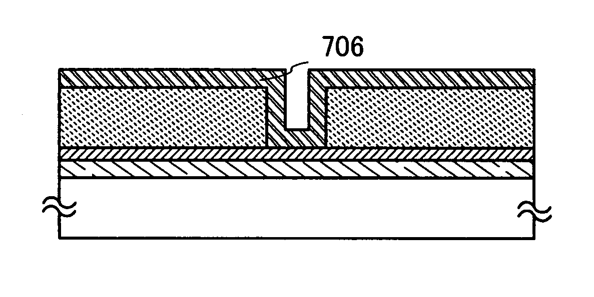
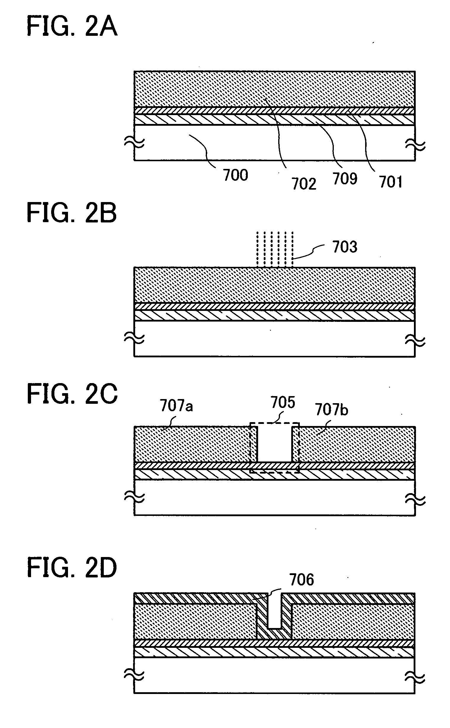
[0080]Description is specifically made with reference to FIGS. 2A to 2D. In this embodiment mode, as shown in FIGS. 2A to 2D, a conductive layer 709, a light absorbing layer 701, and an insulating layer 702 are formed over a substrate 700. In this embodiment mode, the light absorbing layer 701 is formed using a conductive material and can function as a conductive layer. In addition, the conductive layer 709 may be formed using a material that absorbs laser light so that it also functions as a light absorbing layer.

[0081]The conductive layer 709 an...

embodiment mode 3

[0093]In this embodiment mode, a method for manufacturing a display device through a highly reliable and more simplified process at low cost is described with reference to FIGS. 3A to 3C.

[0094]In this embodiment mode, when processing a thin film into a desired pattern, a component (also referred to as a pattern) such as a conductive layer or a semiconductor layer is selectively formed so as to have a desired shape without the use of a photolithography process. In the present invention, a component (also referred to as a pattern) refers to a conductive layer such as a wiring layer, a gate electrode layer, a source electrode layer, or a drain electrode layer, a semiconductor layer, an insulating layer, or the like included in a thin film transistor or a display device and can be any component formed to have a predetermined shape.

[0095]In this embodiment mode, a light absorbing film such as a conductive film or a semiconductor film is formed over a light-transmitting transfer substrate...


PUM


Abstract

An object is to provide a display device that can be manufactured by improvement of use efficiency of a material and simplification of a manufacturing process. A light absorbing layer is formed, an insulating layer is formed over the light absorbing layer, the light absorbing layer and the insulating layer are selectively irradiated with laser light, an irradiated region in the insulating layer is removed to form an opening in the insulating layer, and a conductive film is formed in the opening so as to be in contact with the light absorbing layer. The conductive film is formed in the opening so as to be in contact with the light absorbing layer, which is exposed, so that the light absorbing layer and the conductive layer can be electrically connected with the insulating layer interposed therebetween.

Description

BACKGROUND OF THE INVENTION[0001]1. Field of the Invention[0002]The present invention relates to a method for manufacturing a display device having a stacked-layer structure of thin films, and specifically relates to a processing step of forming a hole in a thin film in a process of manufacturing a display device.[0003]2. Description of the Related Art[0004]Thin film transistors (hereinafter also referred to as TFTs) and an electronic circuit using a thin film transistor are manufactured by stacking of thin films such as semiconductor films, insulating films, or conductive films over a substrate and forming a predetermined pattern as appropriate by a photolithography technique. A photolithography technique is a technique for transferring a pattern of a circuit or the like, which is formed from a light-blocking material on a surface of a transparent planar plate, which is called a photomask, onto a target substrate by utilization of light, and it has been generally used in manufactur...

Claims


Application Information

Patent Timeline
Patent Type & Authority Applications(United States)
IPC IPC(8): H01L21/768H01L33/00
CPCG02F1/136286H01L21/76802H01L21/76838H01L51/5284H01L27/1248H01L51/56H01L2227/323H01L27/124H01L51/529H10K50/87H10K50/865H10K59/1201H10K71/00
Inventor YAMAZAKI, SHUNPEITANAKA, KOICHIROSHOJI, HIRONOBUOISHI, HIROTADA
Owner SEMICON ENERGY LAB CO LTD
Why Eureka
Try Eureka