Method and apparatus for detecting lithographic hotspots

Inactive Publication Date: 2008-09-25
RGT UNIV OF CALIFORNIA
View PDF2 Cites 6 Cited by
  • Summary
  • Abstract
  • Description
  • Claims
  • Application Information

AI Technical Summary

Problems solved by technology

Aggressive technology scaling has introduced new variation sources and made process variation control more difficult.
The primary risk posed by lower k1 is the likelihood of degradation of patterning fidelity on VLSI circuits.
Lower k1 could decrease patterning fidelity and result in generation of many “hotspots.” A hotspot is an actual device pattern which has relatively large critical dimension (CD) and image errors with respect to on-wafer targets.
Hotspots can form under a variety of conditions such as the original design being unfriendly to the resolution enhancement tec

Method used


Image

  • Method and apparatus for detecting lithographic hotspots
  • Method and apparatus for detecting lithographic hotspots
  • Method and apparatus for detecting lithographic hotspots

Examples


Embodiment Construction

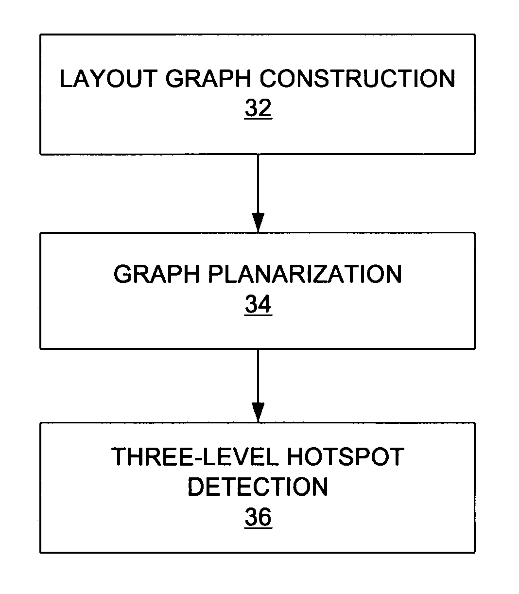
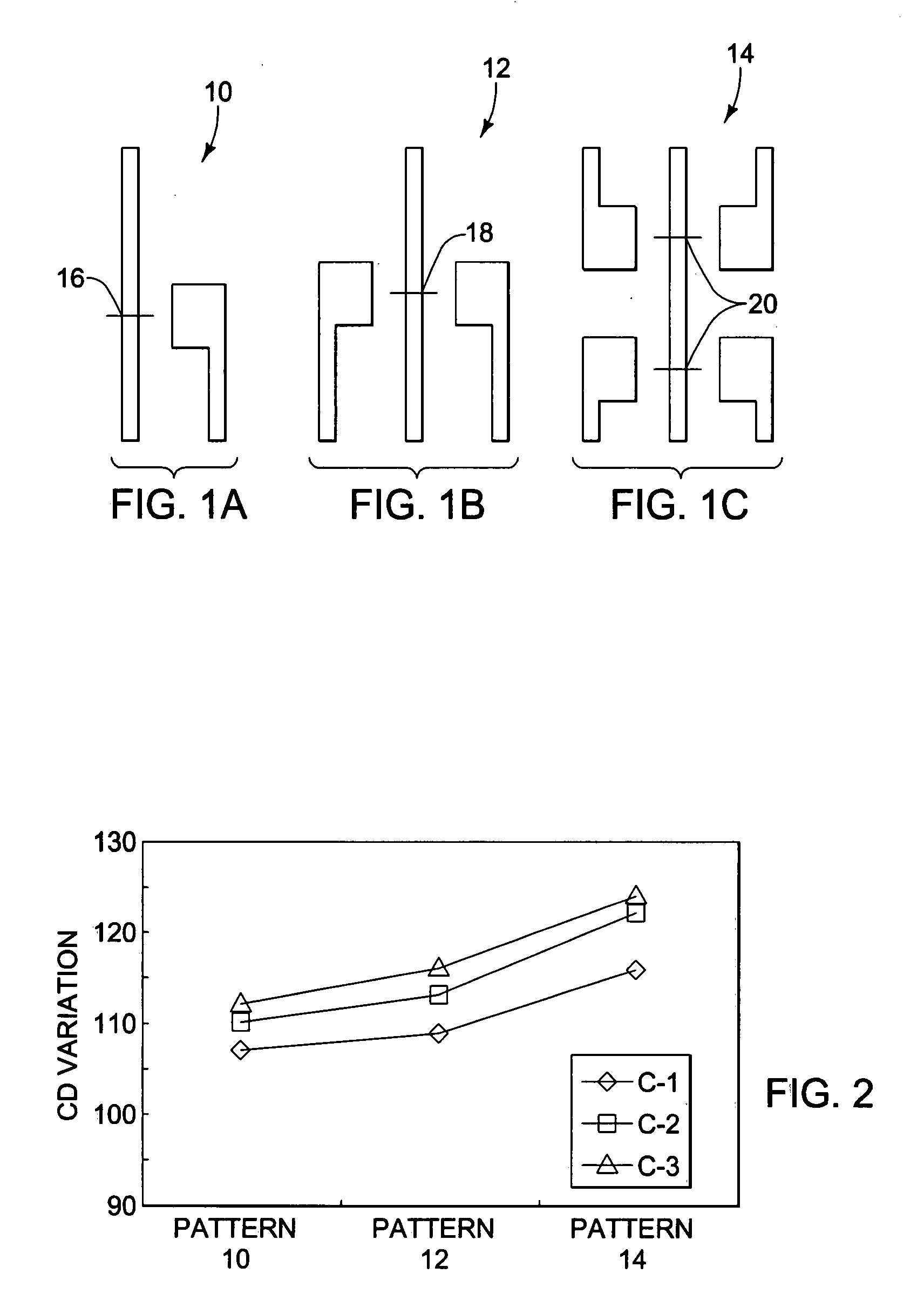
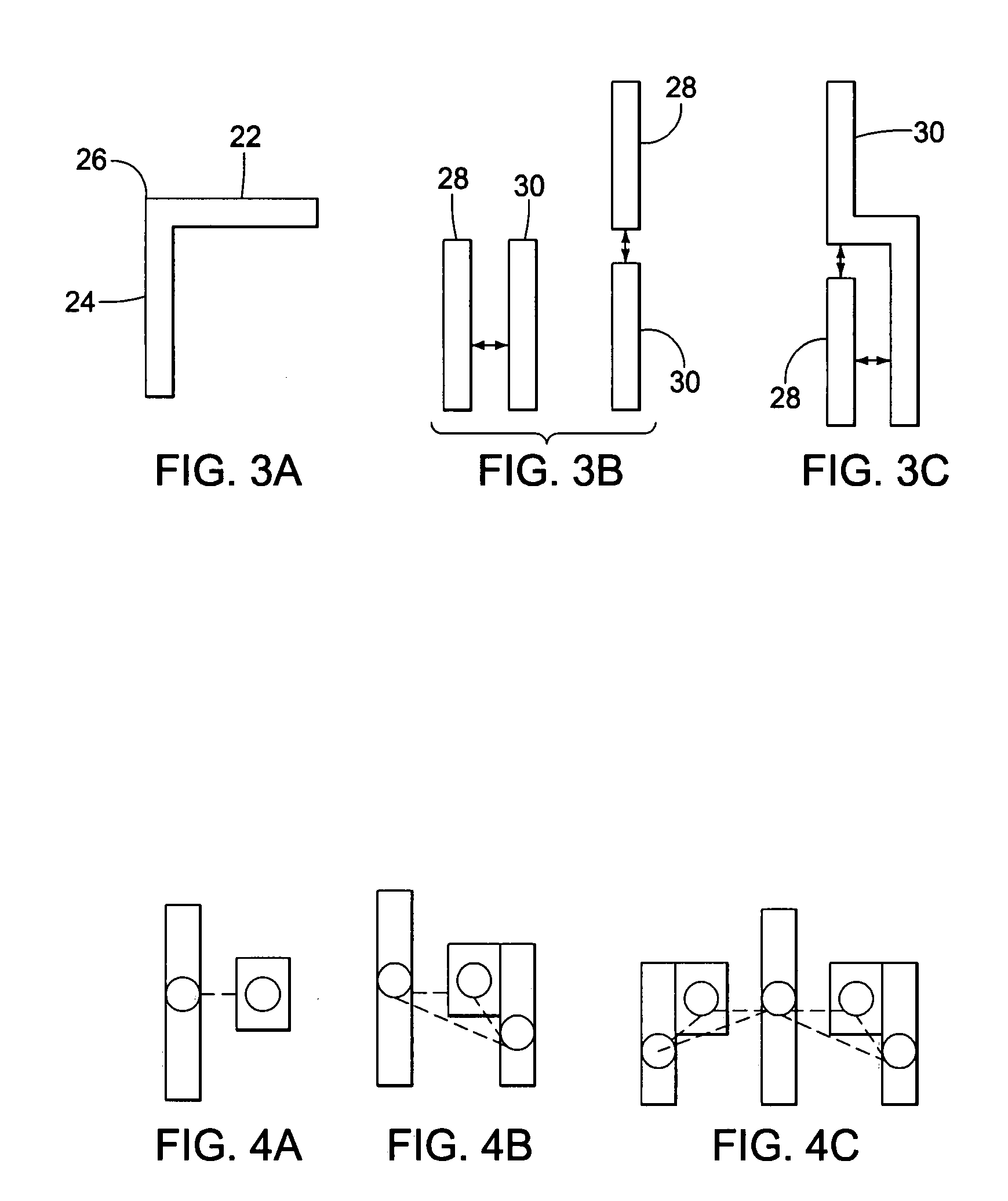
[0018]Briefly, the present invention is directed to a detection method for hotspots induced by lithographic uncertainty. The hotspot detection method includes building a layout graph which reflects pattern-related critical dimension (CD) variation. Given a layout L, the layout graph G=(V, Ec ∪ Ep) consists of nodes V, corner edges Ec and proximity edges Ep between the nodes V. A face in the layout graph includes several close features and the edges between them. The weight given to the edges is calculated from a traditional 2-D model. Then a three-level hotspot detection is applied: (1) edge-level detection finds the hotspot caused by two close features or “L-shaped” features; (2) face-level detection finds the pattern-related hotspots which span several close features; and (3) merged-face-level detection finds hotspots with more complex patterns. To find the merged faces which capture the pattern-related hotspots, the layout is converted into a planar graph G. Then its dual graph G...


PUM


Abstract

Method for detecting hotspots in a circuit layout includes constructing a layout graph having nodes, corner edges and proximity edges from the circuit layout, converting the layout graph to a corresponding dual graph, and iteratively selecting edges and nodes having weights greater than a predetermined threshold value at each iteration as hotspots.

Description

FIELD OF THE INVENTION[0001]The present invention relates to optical lithography, and in particular to a method for detecting hotspots induced by lithographic uncertainties.BACKGROUND OF THE INVENTION[0002]Moore's Law continues to drive higher performance with smaller circuit features. Aggressive technology scaling has introduced new variation sources and made process variation control more difficult. For optical lithography, manufacturability is roughly defined by the k1 factor from the Rayleigh equation. Beyond the 45 nm CMOS technology node, even using a high-end optical exposure system such as immersion lithography with higher numerical aperture (NA), it is necessary to have a k1 factor lower than 0.35. The primary risk posed by lower k1 is the likelihood of degradation of patterning fidelity on VLSI circuits. Lower k1 could decrease patterning fidelity and result in generation of many “hotspots.” A hotspot is an actual device pattern which has relatively large critical dimensio...

Claims


Application Information

Patent Timeline
IPC IPC(8): G06F17/50
CPCG06F17/5081G06F30/398
Inventor KAHNG, ANDREW B.PARK, CHUL-HONGXU, XU
Owner RGT UNIV OF CALIFORNIA
Why Eureka
Try Eureka