Image-sensing module and manufacturing method thereof, and image capture apparatus

Active Publication Date: 2008-10-02
UNITED MICROELECTRONICS CORP
View PDF9 Cites 4 Cited by
  • Summary
  • Abstract
  • Description
  • Claims
  • Application Information

AI Technical Summary

Benefits of technology

[0008]Accordingly, at least one objective of the present invention is to prov

Problems solved by technology

In the conventional technique, the lens group 130 includes a large number of components so that the material cost is high and the assembling time is long.
As a result, the con

Method used


Image

  • Image-sensing module and manufacturing method thereof, and image capture apparatus
  • Image-sensing module and manufacturing method thereof, and image capture apparatus
  • Image-sensing module and manufacturing method thereof, and image capture apparatus

Examples


Example

[0049]Reference will now be made in detail to the present preferred embodiments of the invention, examples of which are illustrated in the accompanying drawings. Wherever possible, the same reference numbers are used in the drawings and the description to refer to the same or like parts.

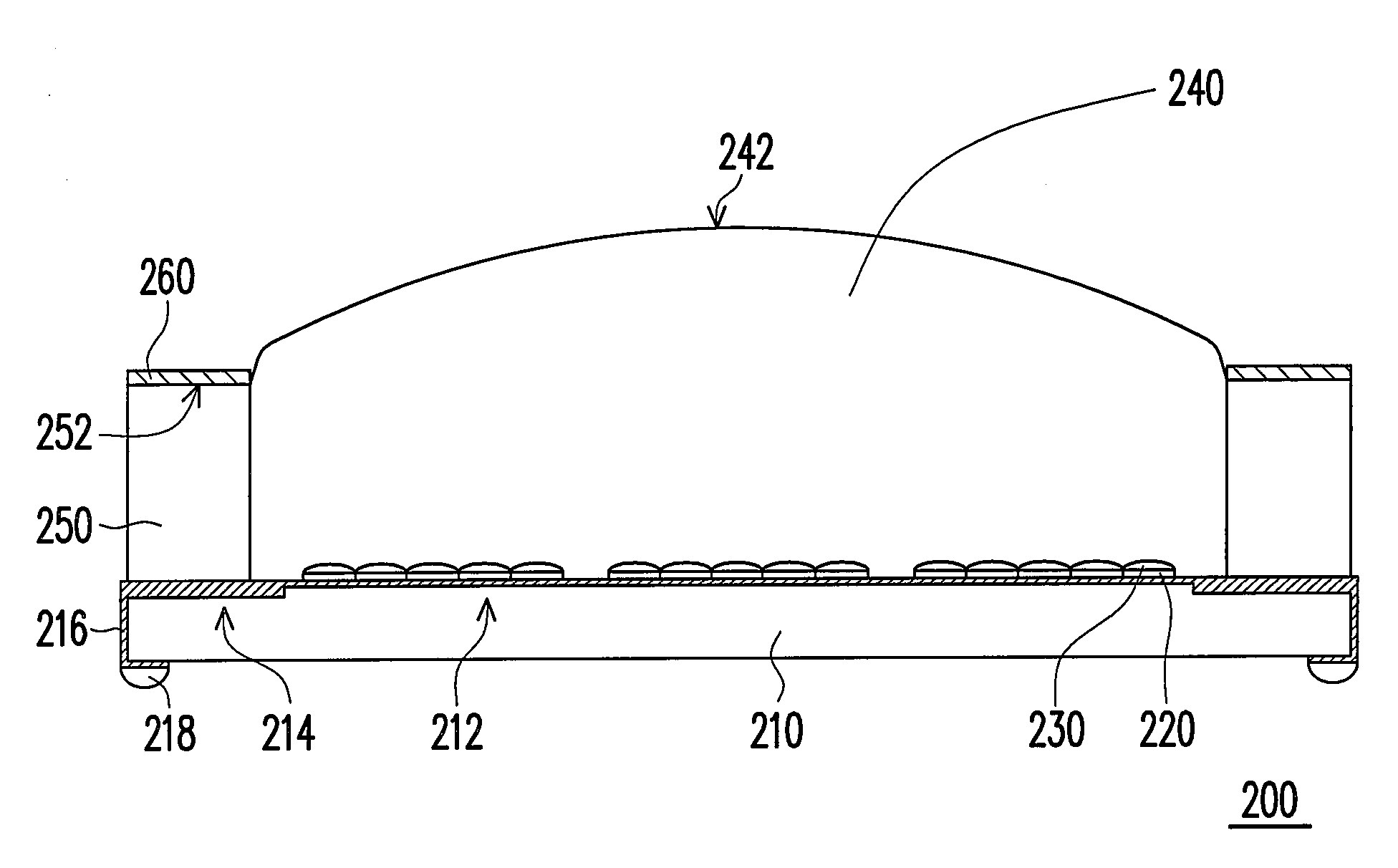
[0050]FIG. 2 is a schematic cross-sectional view of an image-sensing module according to one embodiment of the present invention. As shown in FIG. 2, the image-sensing module 200 in the present embodiment includes a substrate 210, a plurality of image-sensing units 220, a plurality of micro lenses 230 and a focusing unit 240. The image-sensing units 220 are disposed on the substrate 210 and the micro lenses 230 are respectively disposed on one of the image-sensing units 220. The focusing unit 240 is disposed on the substrate 210 and covers the micro lenses 230. A top surface 242 of the focusing unit 240 is a curved surface.

[0051]The substrate 210 in the foregoing image-sensing module 200 is a circuit...


PUM


Abstract

An image-sensing module is provided. The image-sensing module includes a substrate, a plurality of image-sensing units, a plurality of micro lenses and a focusing unit. The image-sensing units are disposed on the substrate and the micro lenses are respectively disposed on one of the image-sensing units. The focusing unit is disposed on the substrate and covers the micro lenses. A top surface of the focusing unit is a curved surface. Furthermore, a method of manufacturing the image-sensing module and an image capture apparatus are provided.

Description

BACKGROUND OF THE INVENTION[0001]1. Field of the Invention[0002]The present invention relates to an image-sensing module, and more particularly, to an image-sensing module with a focusing unit and a manufacturing method thereof, and an image capture apparatus with the image-sensing module.[0003]2. Description of Related Art[0004]The process of fabricating complementary metal-oxide-semiconductor (CMOS) image sensor and CMOS transistor are compatible. Therefore, image sensors along with other peripheral circuits can be easily integrated on the same chip to reduce overall production cost and power consumption. In recent years, CMOS image sensors are widely adopted in low-end applications and frequently serve as a replacement for charge-coupled devices. Consequently, the importance of CMOS image sensors is increasing every day.[0005]FIG. 1A is a schematic diagram of a conventional CMOS image sensor, and FIG. 1B is an explosion view showing the components of the CMOS image sensor in FIG....

Claims


Application Information

Patent Timeline
IPC IPC(8): H04N5/335G02B3/00G03B3/00H01L27/14H04N5/374
CPCH01L27/14618H01L27/14625H01L27/14627H01L27/14685H04N5/2254H04N5/2257H01L2924/0002H04N23/57H04N23/55H01L2924/00
Inventor HSUAN, MIN-CHIHKO, TSUNG-HSICHEN, LI-CHE
Owner UNITED MICROELECTRONICS CORP
Why Eureka
Try Eureka