Structure for one-sample-per-bit decision feedback equalizer (DFE) clock and data recovery

a one-sample-per-bit decision feedback equalizer and data recovery technology, applied in the direction of pulse manipulation, pulse technique, digital transmission, etc., can solve the problem of increasing the bit error rate (ber), key source of complexity in equalization-based receivers is the number of samples per bit, etc., to reduce the bit error rate (ber) and maintain the peak energy

Inactive Publication Date: 2008-10-02
GLOBALFOUNDRIES INC
View PDF15 Cites 17 Cited by
  • Summary
  • Abstract
  • Description
  • Claims
  • Application Information

AI Technical Summary

Benefits of technology

[0010]Disclosed is a receiver circuit, method and design architecture of a decision feedback equalizer (DFE) Clock-And-Data Recovery (CDR) architecture that utilizes / produces one sample-per-bit in the receiver and reduces bit-error-rate (BER). The method and circuit design combines an integrating receiver with a decision feedback equalizer along with the appropriate (CDR) loop with peak detector (i.e., whereby the phase error is smallest when the peak is maximum) to maintain a single sample per bit requirement. This configuration enables performance of an eye centering algorithm, which maintains the peak energy. The output power (energy) of the latch is maximized to obtain the correct phase by performing integration in front of the data latch in order to provide necessary amplification. The integration collects the energy required to switch the latch and further enables alignment of the phases.
[0012]The incoming voltage is converted to a current and connected to a current summing node. Weighted currents determined by the values of previously detected bits and their respective feedback coefficients are also connected to this node. Then, the sum of all currents is integrated and converted to a voltage. A sampler is then utilized to make a bit decision based on this resulting voltage. After sampling, the integrator is reset before analysis of the next bit. A delay stage is provided and stores a number of previously-detected bits which are connected through the weighted voltage coefficient to feedback current converters. A peak detector is connected to the output of the current integrator, and the value of the peak detector is maximized in the CDR loop by adjusting the sampling clock phase.

Problems solved by technology

These non-ideal conditions within the channel causes inter-symbol-interference (ISI), leading to timing uncertainties at the receiver and an increase in the bit error rate (BER).
It is not a coincidence therefore, that one of the key sources of complexity in equalization-based receivers is the number of samples per bit utilized.
While conventional integration methods have been implemented to attempt to overcome this requirement, there still exists a problem with conventional integration in that a very small value may be obtained if the timing is wrong.

Method used


Image

  • Structure for one-sample-per-bit decision feedback equalizer (DFE) clock and data recovery
  • Structure for one-sample-per-bit decision feedback equalizer (DFE) clock and data recovery
  • Structure for one-sample-per-bit decision feedback equalizer (DFE) clock and data recovery

Examples


Embodiment Construction

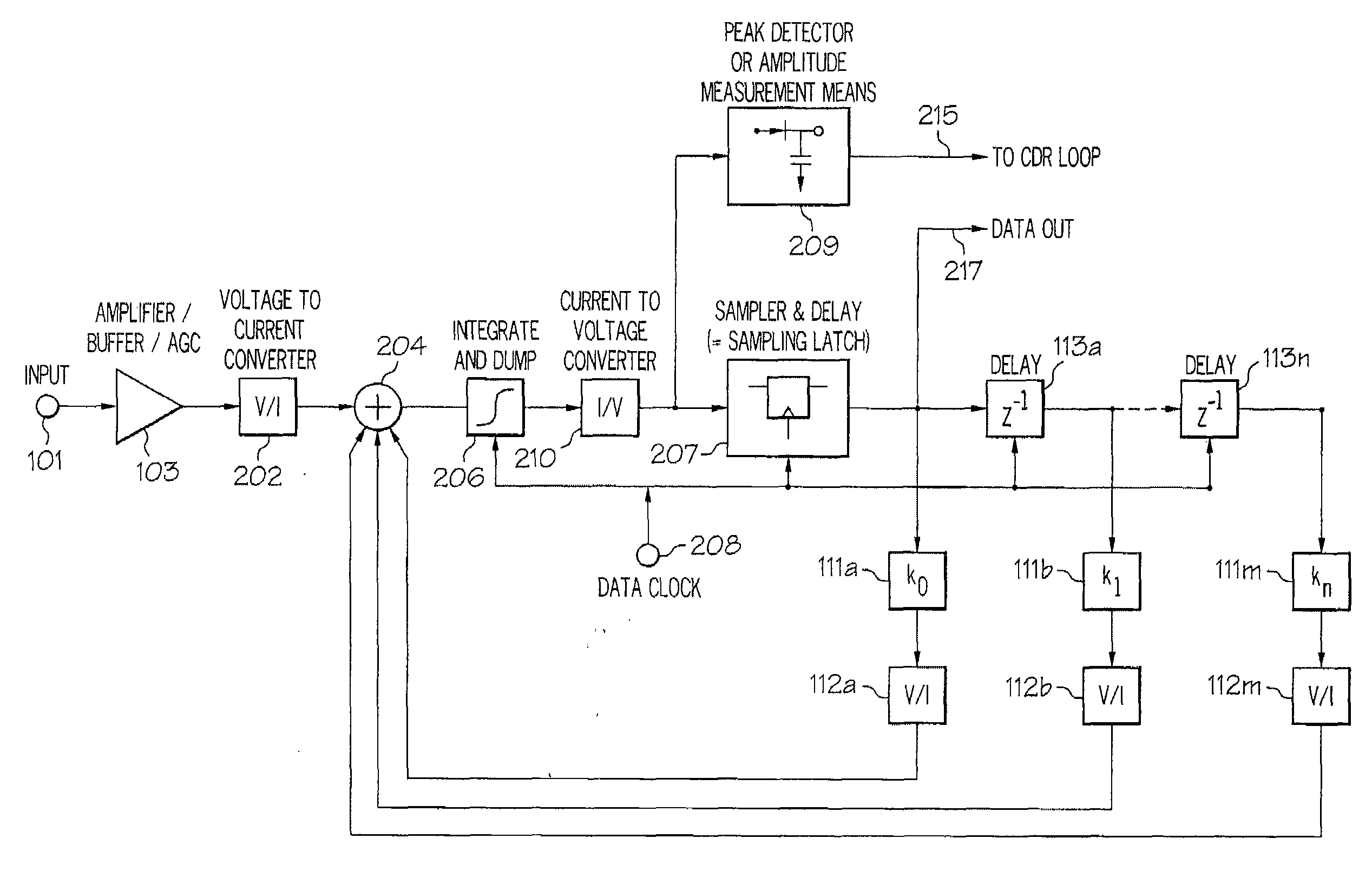
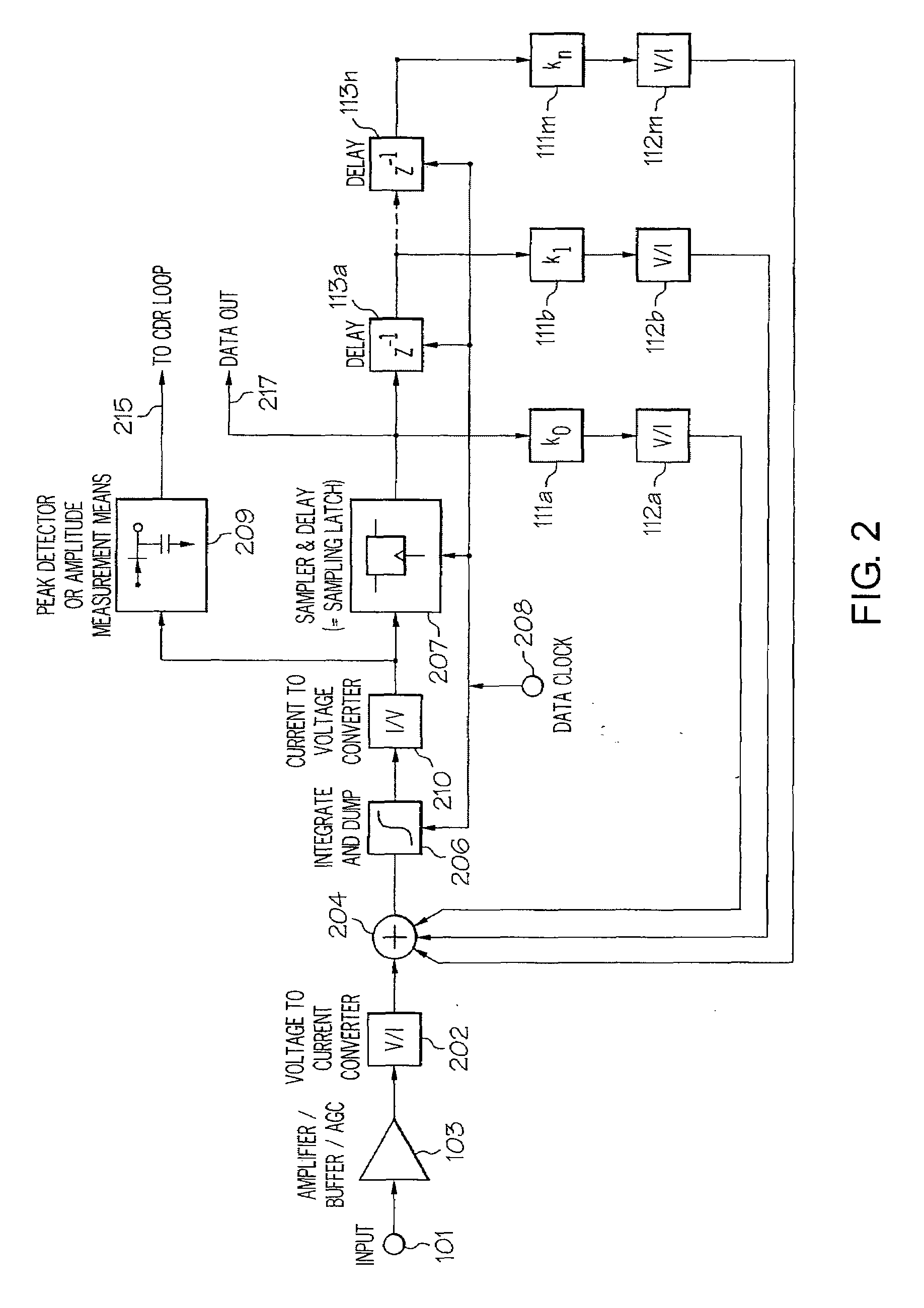
[0020]The present invention provides a receiver circuit, method and design architecture of a decision feedback equalizer (DFE) Clock-And-Data Recovery (CDR) architecture that utilizes / produces one sample-per-bit in the receiver and reduces bit-error-rate (BER).

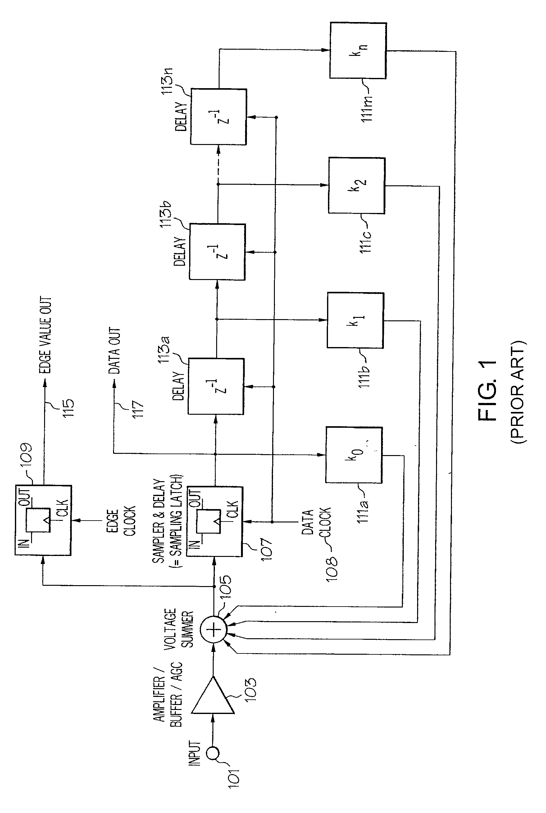
[0021]With reference now to the figures, and in particular with reference to FIG. 2, which illustrate a circuit design of the enhanced DFE architecture, according to one embodiment of the invention. Within the descriptions of the figures, (i.e., relative to previously described FIG. 1) similar elements are provided similar names and reference numerals as those of the previous figure. Where the later figure utilizes the element in a different context or with different functionality, the element is provided a different leading numeral representative of the figure number (e.g, 1xx for FIG. 1 and 2xx for FIG. 2). The specific numerals assigned to the elements are provided solely to aid in the description and not meant to imply any...


PUM


Abstract

A design structure embodied in a machine readable storage medium for designing, manufacturing, and / or testing a design of a decision feedback equalizer (DFE) Clock-And-Data Recovery (CDR) architecture that utilizes / produces one sample-per-bit in the receiver and reduces bit-error-rate (BER) is provided. The design generally includes a receiver circuit. The receiver circuit generally includes a decision feedback equalizer (DFE) that produces one sample per bit, and means for automatically self-adjusting the DFE to enable an eye centering process by which peak energy is maintained within the receiver circuit when phase error is a minimum.

Description

CROSS-REFERENCE TO RELATED APPLICATION[0001]This application is a continuation-in-part of co-pending U. S. patent application Ser. No. 11 / 405,997, filed Apr. 18, 2006, which is herein incorporated by reference.BACKGROUND OF THE INVENTION[0002]1. Field of the Invention[0003]The present invention relates generally to design structures, and more specifically, design structures for electric circuits and in particular to data receivers. Still more particularly, the present invention relates to equalization-based data receivers.[0004]2. Description of the Related Art[0005]Most modern data transmission relies on high-speed input / output (I / O) electrical data transmission channels linking a data transmitter (or transceiver) and a data receiver (i.e., the receiving circuit of a transceiver). Typically, this channel has a nonlinear frequency / phase response due to non-ideal conditions, which affect (e.g., distorts, attenuates, etc.) the transmitted data propagating through the channel. These no...

Claims


Application Information

Patent Timeline
Patent Type & Authority Applications(United States)
IPC IPC(8): H04L27/01
CPCH04L25/03057H04L25/03885H04L2025/03356
Inventor CARBALLO, JUAN A.CRANFORD, HAYDEN C.NICHOLLS, GARETH J.NORMAN, VERNON R.SCHMATZ, MARTIN L.
Owner GLOBALFOUNDRIES INC
Why Eureka
Try Eureka