Methods for forming a photovoltaic device with low contact resistance

a photovoltaic device and microcrystalline silicon technology, applied in the manufacture of final products, basic electric elements, coatings, etc., can solve the problems of low photoelectric conversion efficiency, high contact barrier, device failure, etc., and achieve the effect of high photoelectric conversion efficiency and low contact resistan

Inactive Publication Date: 2008-10-09
APPLIED MATERIALS INC
View PDF98 Cites 35 Cited by
  • Summary
  • Abstract
  • Description
  • Claims
  • Application Information

AI Technical Summary

Problems solved by technology

Poor electrical properties of the interfacial contact may result in low photoelectric conversion efficiency and high contact barrier, thereby causing device failure and high power consumption of the PV solar cells.

Method used


Image

  • Methods for forming a photovoltaic device with low contact resistance
  • Methods for forming a photovoltaic device with low contact resistance
  • Methods for forming a photovoltaic device with low contact resistance

Examples


Embodiment Construction

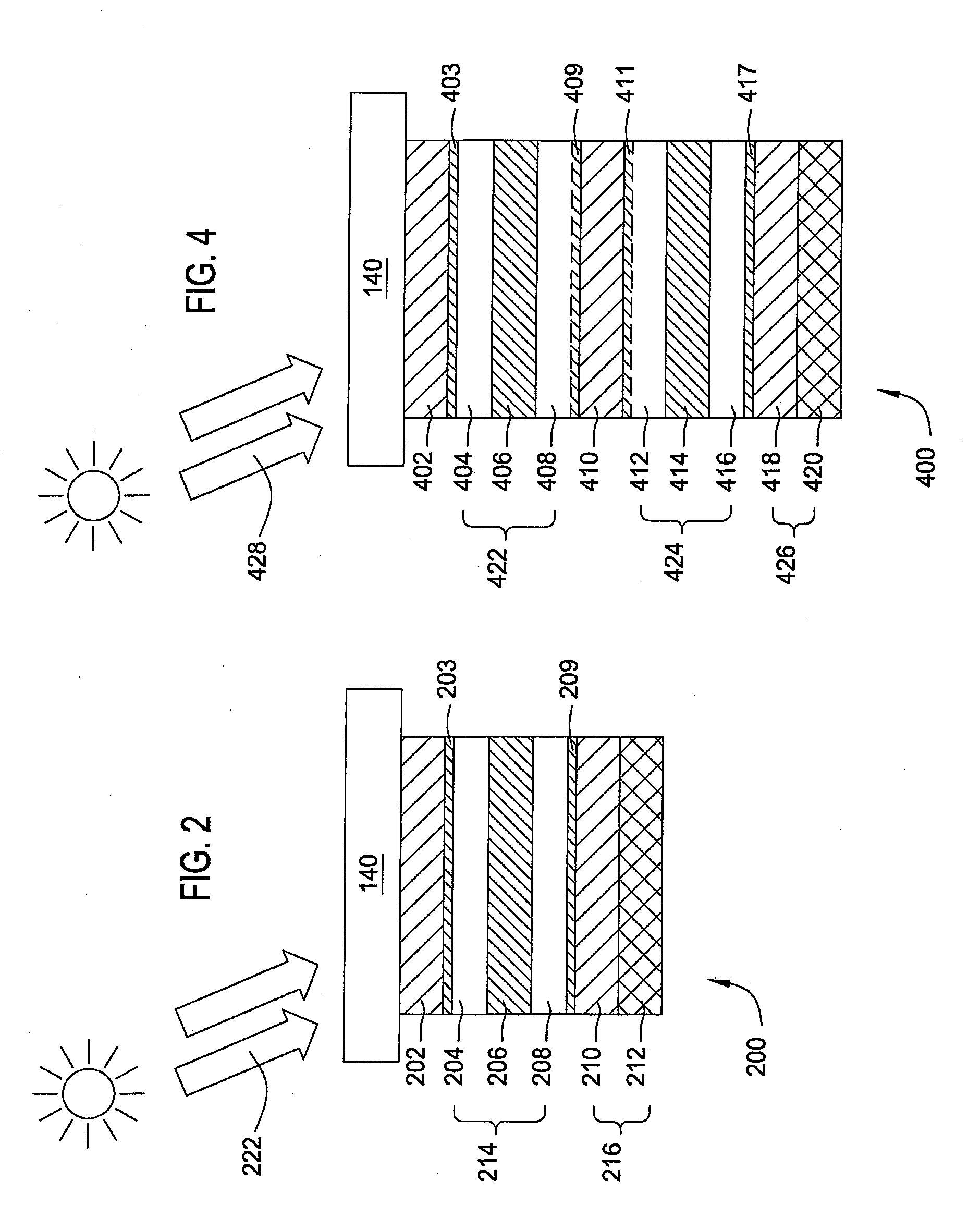
[0021]The present invention provides a structure of a PV solar cell with low contact resistance and high photoelectric conversion efficiency and methods for manufacturing the same. In one embodiment, a microcrystalline silicon (μc-Si) layer is disposed between an amorphous silicon (a-Si) based photoelectric conversion unit and a TCO layer to enhance the electrical properties of interfacial contact between the photoelectric conversion unit and the TCO layer.

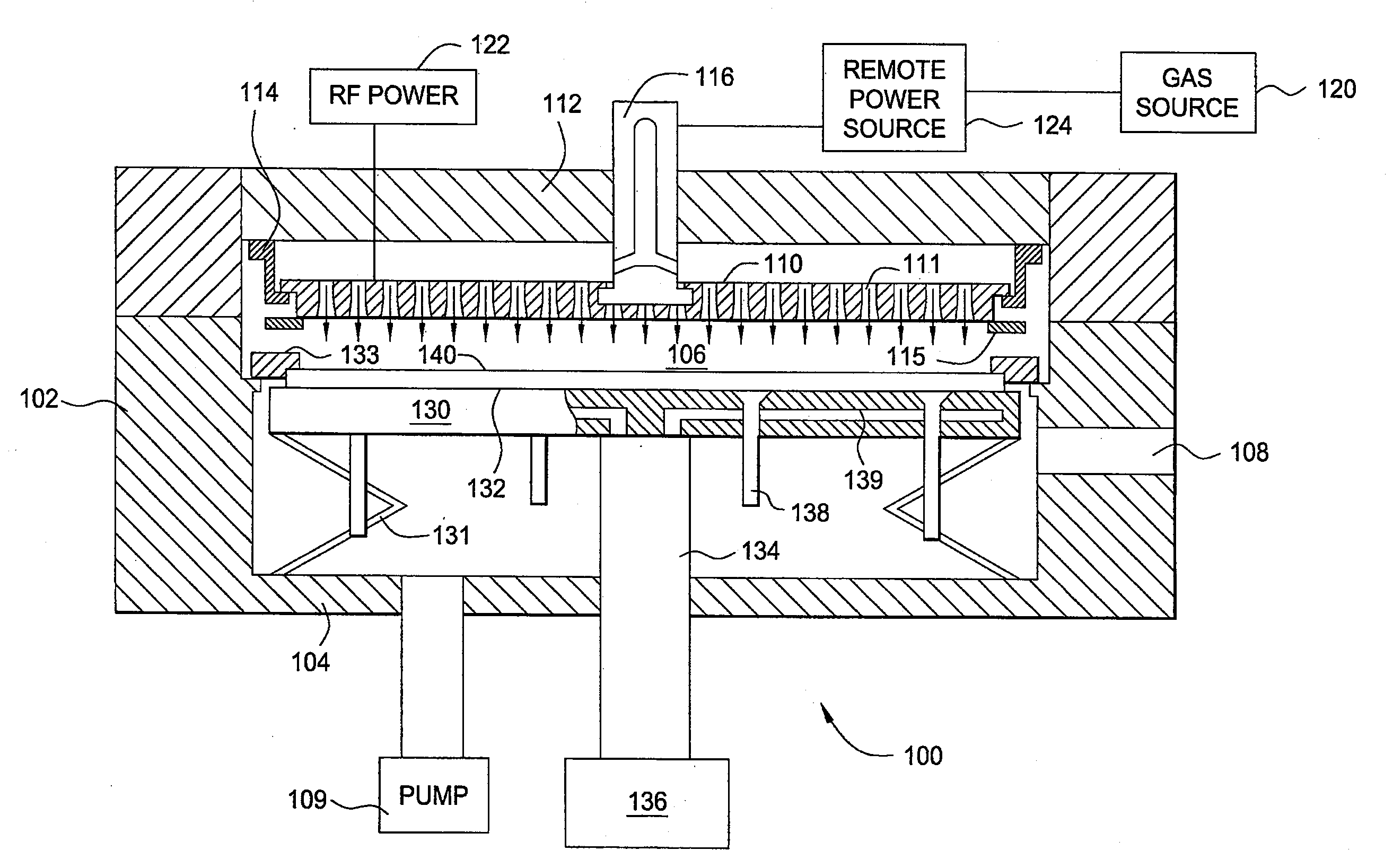
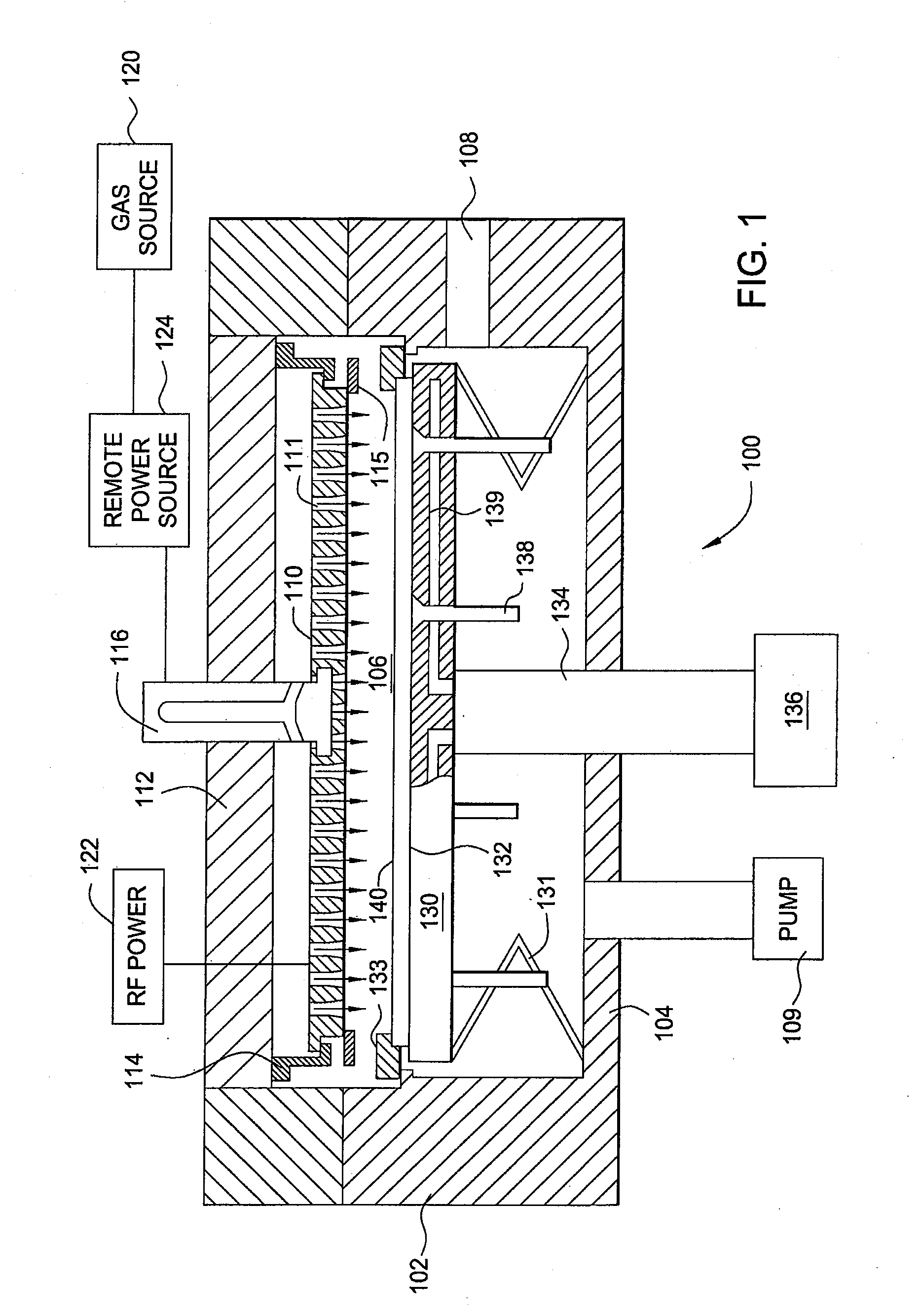
[0022]FIG. 1 is a schematic cross-section view of one embodiment of a plasma enhanced chemical vapor deposition (PECVD) chamber 100 in which one or more films of a solar cell. One suitable plasma enhanced chemical vapor deposition chamber is available from Applied Materials, Inc., located in Santa Clara, Calif. It is contemplated that other deposition chambers, including those from other manufacturers, may be utilized to practice the present invention.

[0023]The chamber 100 generally includes walls 102, a bottom 104, a showerhead 1...


PUM


Abstract

An improved PV solar cell structure and methods for manufacturing the same are provided. In one embodiment, a photovoltaic device includes a first photoelectric conversion unit, a first transparent conductive oxide layer and a first microcrystalline silicon layer disposed between and in contact with the photoelectric conversion unit and the transparent conductive oxide layer. In another embodiment, a method of forming a photovoltaic solar cell includes providing a substrate having a first transparent conductive oxide layer disposed thereon, depositing a first microcrystalline silicon layer on the transparent conductive oxide layer, and forming a first photoelectric conversion unit on the microcrystalline silicon layer.

Description

CROSS-REFERENCE TO RELATED APPLICATIONS[0001]This application is related to U.S. patent application Ser. No. 11 / 624,677, entitled “MULTI-JUNCTION SOLAR CELLS AND METHODS AND APPARATUS FOR FORMING THE SAME,” filed on Jan. 18, 2007, which is herein incorporated by reference in its entirety.BACKGROUND OF THE DISCLOSURE[0002]1. Field of the Invention[0003]The present invention relates to methods for forming a microcrystalline silicon film for photovoltaic devices.[0004]2. Description of the Background Art[0005]Photovoltaic devices (PV) or solar cells are devices which convert sunlight into direct current (DC) electrical power. PV or solar cells typically have one or more p-i-n junctions. Each junction comprises two different regions within an i-type semiconductor material where one side is denoted as the p-type region and the other as the n-type region. When the p-i-n junction of the PV cell is exposed to sunlight (consisting of energy from photons), the sunlight is directly converted t...

Claims


Application Information

Patent Timeline
Patent Type & Authority Applications(United States)
IPC IPC(8): H01L31/00
CPCH01L31/022425H01L31/0745H01L31/076H01L31/077H01L31/1824H01L31/202Y02E10/545Y02E10/548Y02E10/547Y02P70/50H01L31/04
Inventor SHENG, SHURANCHAE, YONG KEEWON, TAE KYUNGLI, LIWEICHOI, SOO YOUNGLI, YANPINGCRUZ, JOE GRIFFITH
Owner APPLIED MATERIALS INC
Why Eureka
Try Eureka