Slew-rate controlled pad driver in digital CMOS process using parasitic device cap

Active Publication Date: 2008-10-09
TEXAS INSTR INC
View PDF2 Cites 18 Cited by
  • Summary
  • Abstract
  • Description
  • Claims
  • Application Information

AI Technical Summary

Benefits of technology

[0005]The present invention is a slew-rate controlled driver circuit in an integrated circuit fabricated in a low voltage CMOS process, having an input node and an output node. A PMOS pull-up transistor is provided, having a source connected to one side of a power supply, having a gate, and having a drain connected to the output node. The PMOS transistor also has a parasitic capacitance between its gate and drain, having a value that may vary from one integrated circuit to the next from process variations and in response to varying circuit conditions.

Problems solved by technology

This creates a challenge for high-speed I/O circui

Method used


Image

  • Slew-rate controlled pad driver in digital CMOS process using parasitic device cap
  • Slew-rate controlled pad driver in digital CMOS process using parasitic device cap
  • Slew-rate controlled pad driver in digital CMOS process using parasitic device cap

Examples


Embodiment Construction

[0021]The making and use of the various embodiments are discussed below in detail. However, it should be appreciated that the present invention provides many applicable inventive concepts which can be embodied in a wide variety of specific contexts. The specific embodiments discussed are merely illustrative of specific ways to make and use the invention, and do not limit the scope of the invention.

[0022]Prior to the detailed disclosure of specific embodiments of the invention, a brief discussion follows of additional background that places the novelty and benefits of the invention in better context.

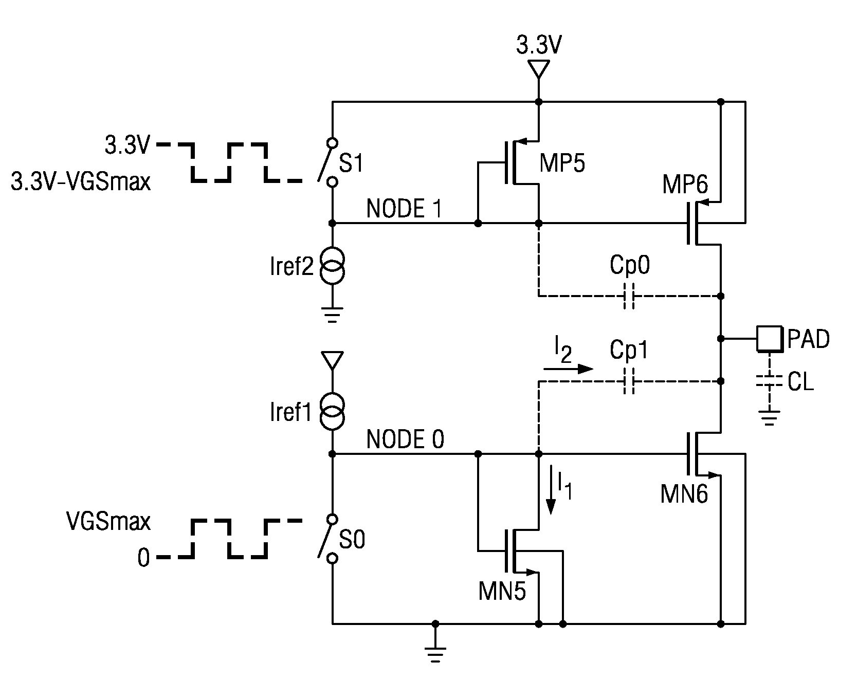
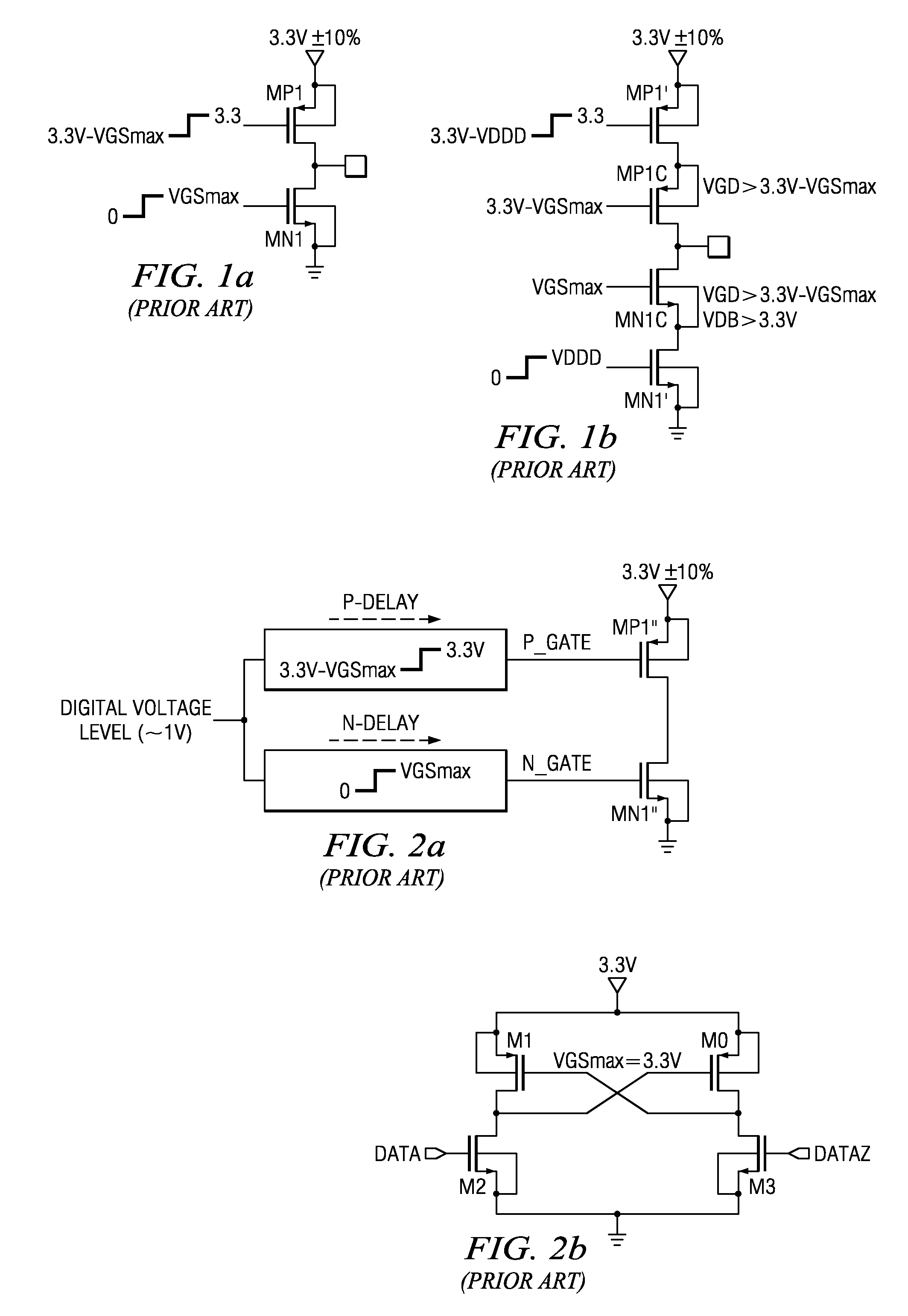
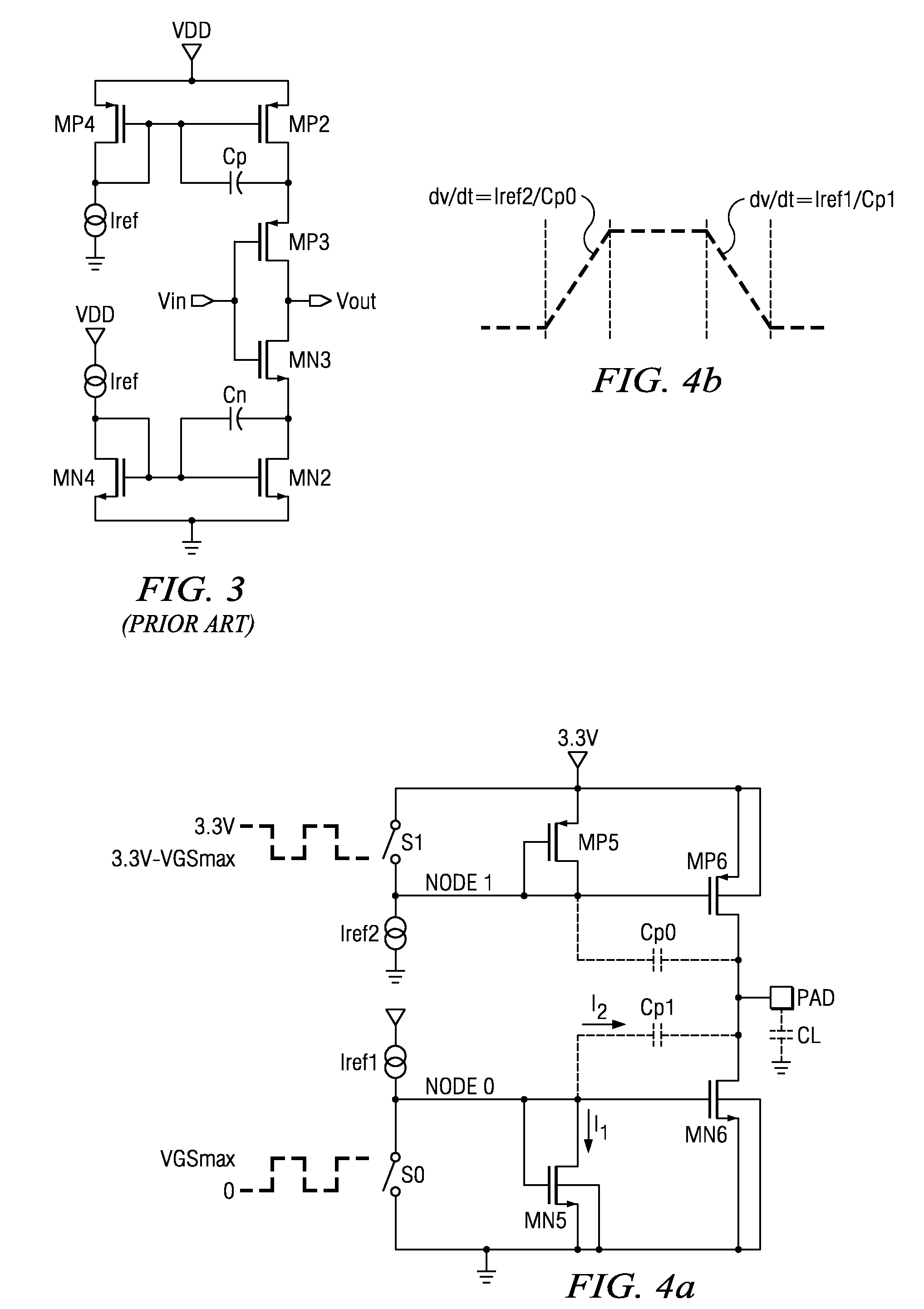
[0023]FIG. 2(a) shows the basic architecture of a simple pad driver, implemented in an integrated circuit fabricated using a low voltage semiconductor process. The N-delay path of the input signal to NMOS device MN1″ and the P-delay path of the input signal to PMOS device MP1″ are preferably matched, to minimize the through current and duty cycle distortion. The delay variation is more do...


PUM


Abstract

A slew-rate controlled driver circuit in an integrated circuit fabricated in a low voltage CMOS process, having an input node and an output node. A PMOS pull-up transistor is provided, having a source connected to one side of a power supply, having a gate, and having a drain connected to the output node. The PMOS transistor also has a parasitic capacitance between its gate and drain, having a value that may vary from one integrated circuit to the next from process variations and in response to varying circuit conditions. A current source generates a current having a level corresponding to the value of the parasitic capacitance, and to provide that current to the gate of the PMOS transistor. A level shifter receives an input signal having a voltage varying in a first range provides as output signal to the gate of the PMOS transistor shifted to a level suitable for the PMOS transistor. An NMOS pull-down transistor is also provided, connected to the other side of the power supply, with a similar and corresponding current source and level shifter as has the PMOS transistor.

Description

TECHNICAL FIELD OF THE INVENTION[0001]The present invention relates to slew-rate controlled driver circuits, and more particularly relates to such drivers in low voltage CMOS processes.BACKGROUND OF THE INVENTION[0002]In many general purpose input / output interfaces, such as USB Multimedia Card I / O (MMCIO), it is required to provide, via CMOS circuitry, a signal that varies between 0 volts and 3.3 volts and has a controlled rise / fall time to reduce electromagnetic interference (EMI) and supply / ground noise. However, deep submicron technology scales transistor voltages, for example by scaling down threshold voltage, VT, and increasing drive to have a lower gate-to-source voltage (“VGS”), supporting lower supply voltages. This creates a challenge for high-speed I / O circuit designs that require a high output voltage swing.[0003]FIG. 1(a) shows basic driver structures and the voltage level the driver transistors need to tolerate. FIG. 1(a) shows a simple driver with single PMOS transisto...

Claims


Application Information

Patent Timeline
IPC IPC(8): H03K19/0185
CPCH03K19/01721
Inventor SETH, SUMANTRAGOEL, ANKUSH
Owner TEXAS INSTR INC
Why Eureka
Try Eureka