Solder pad and method of making the same

Active Publication Date: 2008-10-16
NAN YA PRINTED CIRCUIT BOARD CORPORATION
View PDF8 Cites 10 Cited by
  • Summary
  • Abstract
  • Description
  • Claims
  • Application Information

AI Technical Summary

Benefits of technology

[0010]It is one object of the present invention to provide an improve

Problems solved by technology

It is a major challenge to improve the stability, reliability and yield of both the product and the fabrication process, reduce the cost, and concurrently increase the trace density of the packaging substrate.
The amount of solder paste squeezed into the shrunk S/R opening becomes inadequate and can not contact with the solder pad at the bottom of the S/R opening.
This results in d

Method used


Image

  • Solder pad and method of making the same
  • Solder pad and method of making the same
  • Solder pad and method of making the same

Examples


Embodiment Construction

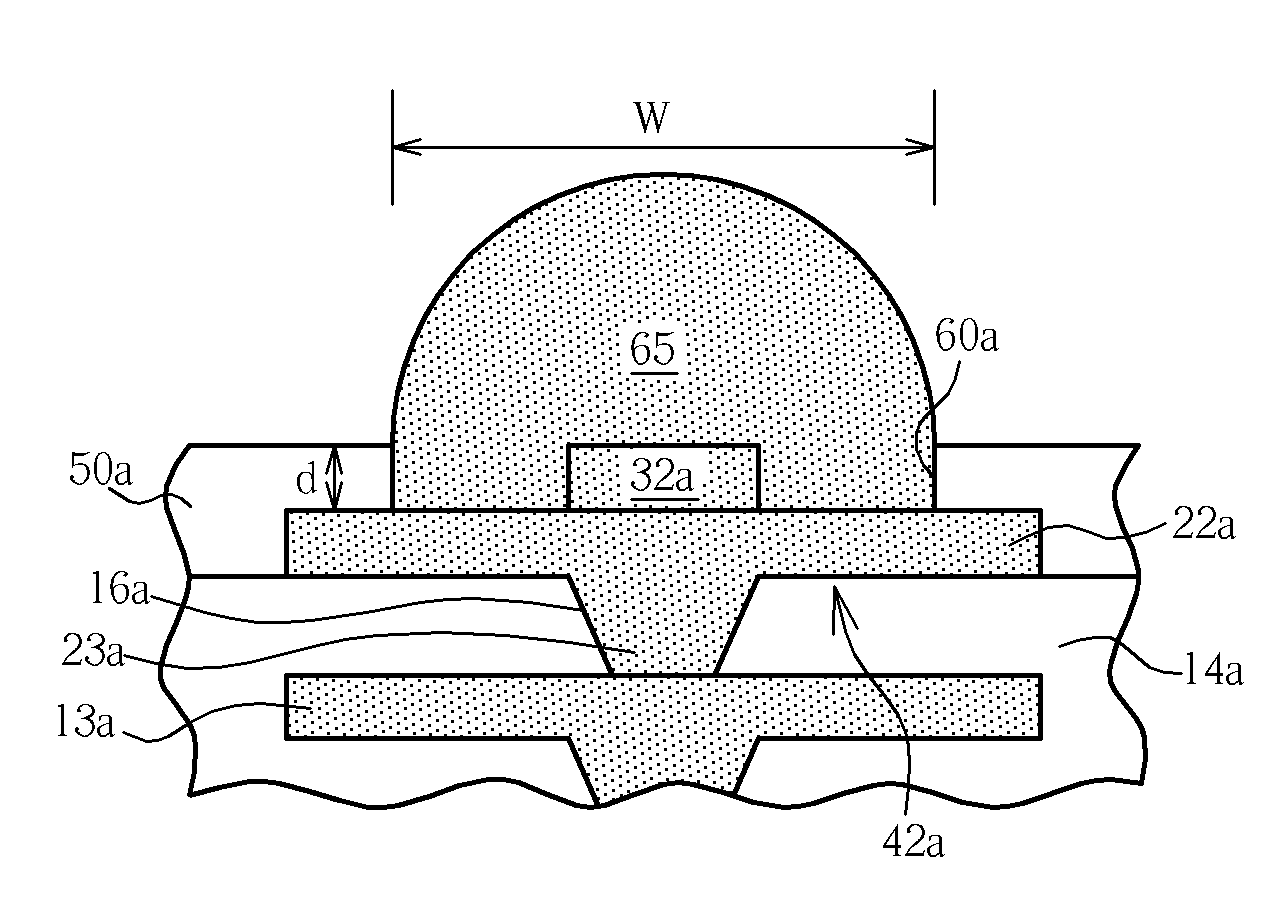
[0017]The present invention pertains to an improved back end process for fabricating packaging substrates. The back end process includes solder paste printing on solder pads and subsequent re-flow process to form solder balls that are firmly and steadily connected to the solder pads.

[0018]The present invention can resolve the prior art problems of small solder resist (S / R) opening and inadequate solder paste squeezed into the S / R opening. The inadequate solder paste in the S / R opening is the root cause of ball falling out and contact failure during the re-flow process. The present invention can improve the product yield.

[0019]The present invention also provides an improved solder pad structure which is capable of firmly connecting with the solder ball and prevents the prior art problems of small solder resist (S / R) opening and contact failure in the S / R opening.

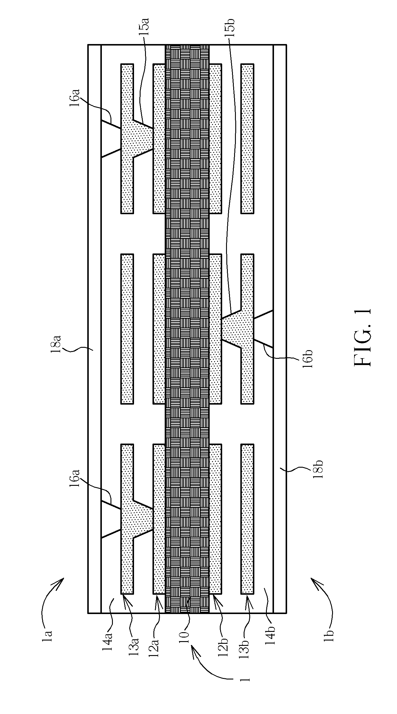
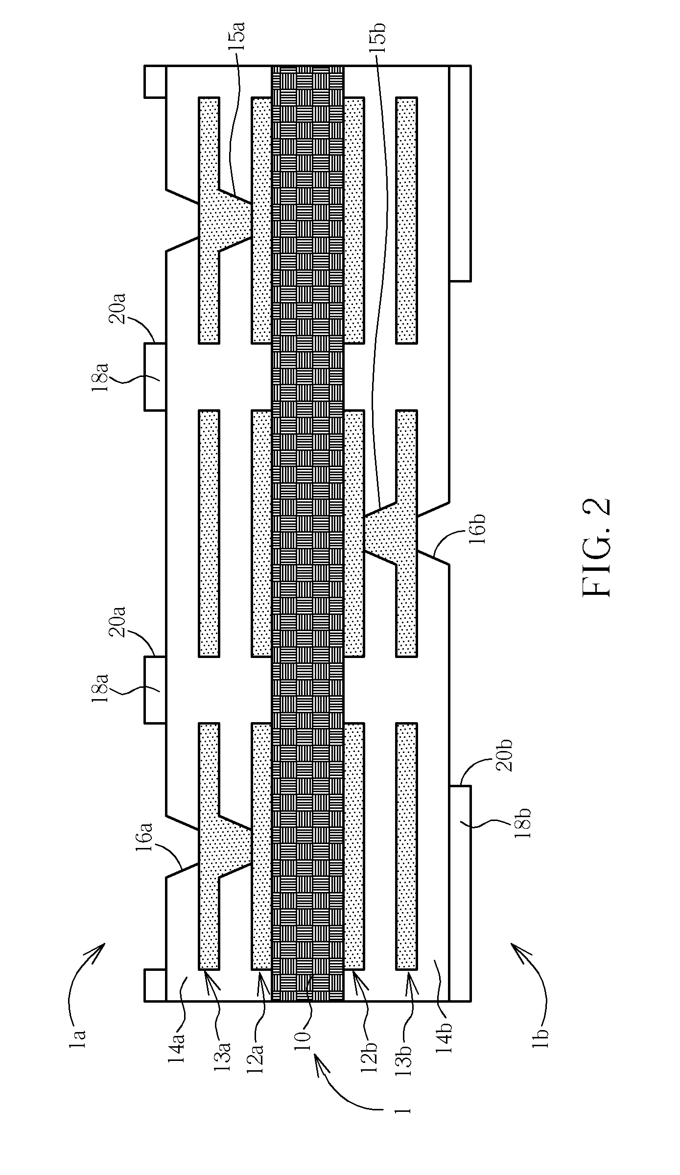
[0020]Please refer to FIGS. 1-10. FIGS. 1-10 are schematic, cross-sectional diagrams illustrating the back end process for ...


PUM


Abstract

A solder pad structure includes a first metal layer disposed on an insulation layer, wherein the first metal layer is electrically connected with an underlying interconnection circuit layer through a conductive through hole disposed in the insulation layer. A solder resist layer having an opening exposing a central portion of the first metal layer is disposed on the insulating layer. A pillar-shaped second metal layer is disposed within the opening directly on the first metal layer. A solder ball filled into the opening is in contact with the pillar-shaped second metal layer.

Description

BACKGROUND OF THE INVENTION[0001]1. Field of the Invention[0002]The present invention relates generally to the field of packaging substrate. More particularly, the present invention relates to a solder pad structure provided on the chip side of a packaging substrate and fabrication method thereof, which is capable of improving solderjoint reliability of the solder ball.[0003]2. Description of the Prior Art[0004]The current trend toward lighter, thinner and smaller electronic products has driven the market to pay more attention to the flip chip packaging technology. The flip chip technology has several advantages over the conventional packaging approaches and has thus become the mainstream in the packaging and testing industry. As the high-level ball type packaging such as ball grid array (BGA) or flip chip is widely employed, the demand for the packaging substrate thereof is increased.[0005]The trace or circuit on the surface of the packaging substrate has become denser and denser. ...

Claims


Application Information

Patent Timeline
IPC IPC(8): H01L23/48
CPCH01L23/498H01L23/49816H01L2924/0002H05K1/113H05K3/108H05K3/243H05K3/3452H05K3/3457H05K3/4007H05K3/4644H05K2201/0367H05K2201/09563H05K2201/099H05K2203/0574H01L2924/00
Inventor CHU, CHIH-CHUNGLIN, SHIH-TSUNGLIN, HSIEN-CHIEH
Owner NAN YA PRINTED CIRCUIT BOARD CORPORATION
Why Eureka
Try Eureka