Thin film transistor, method of manufacturing the same, and flat panel display having the same

a technology of thin film transistors and flat panels, applied in the direction of basic electric elements, semiconductor devices, electrical equipment, etc., can solve the problems of limited improvement of device characteristics, complicated manufacturing process, and very sensitive color to current stress, so as to increase the stability of driving each pixel and uniform device characteristics

Active Publication Date: 2008-10-23
SAMSUNG ELECTRONICS CO LTD
View PDF12 Cites 4020 Cited by
  • Summary
  • Abstract
  • Description
  • Claims
  • Application Information

AI Technical Summary

Benefits of technology

[0015]To solve the above and/or other problems, the present invention provides a thin film transistor (TFT) that ensure

Problems solved by technology

However, the color is very sensitive to current stress.
However, even though the compensation circuit is configured, the improvement of

Method used


Image

  • Thin film transistor, method of manufacturing the same, and flat panel display having the same
  • Thin film transistor, method of manufacturing the same, and flat panel display having the same
  • Thin film transistor, method of manufacturing the same, and flat panel display having the same

Examples


Embodiment Construction

[0046]A thin film transistor (TFT) according to the present invention, a method of manufacturing the TFT, and a flat panel display having the TFT will now be described more fully with reference to the accompanying drawings in which exemplary embodiments of the invention are shown. In the drawings, the thicknesses of layers and regions are exaggerated for clarity.

[0047]First, the TFT according to an embodiment of the present invention will now be described.

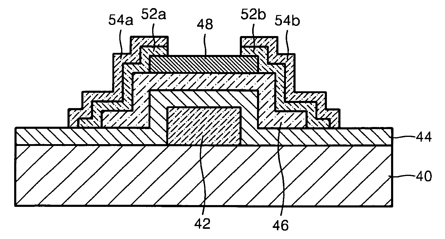
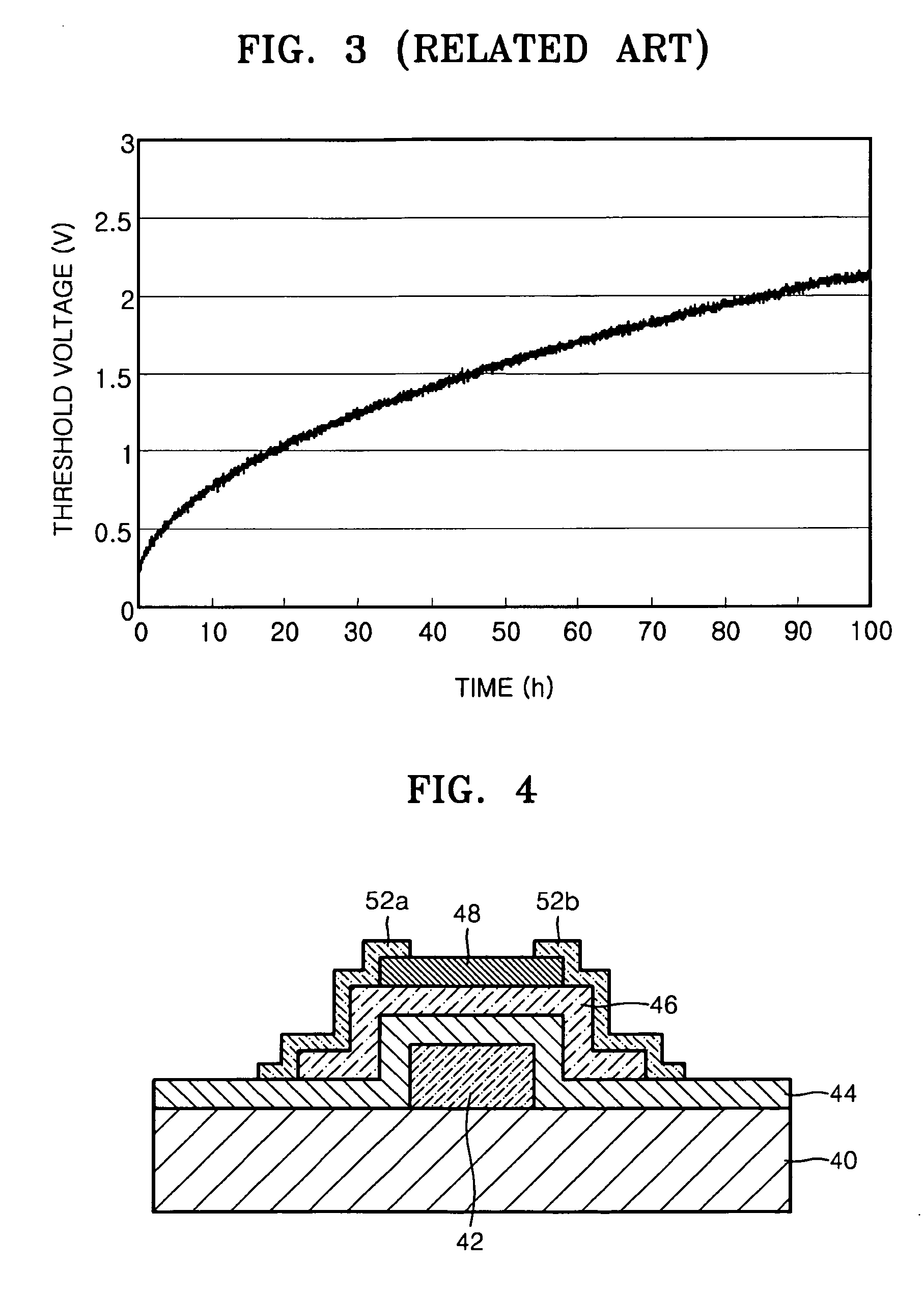
[0048]FIG. 4 is a cross-sectional view of a TFT according to an embodiment of the present invention. Referring to FIG. 4, a gate 42 is formed on a substrate 40. The substrate 40 can be an insulating substrate, for example, a glass substrate. The gate 42 can be a single layer or a multiple layer. If the gate 42 is a single layer, the gate 42 can be a Mo layer or another metal layer different from the Mo layer. If the gate 42 is a multiple layer, the gate 42 can be a layer in which two or three metal layers are sequentially stacked. ...


PUM


Abstract

A thin film transistor (TFT), a method of manufacturing the TFT, and a flat panel display comprising the TFT are provided. The TFT includes a gate, a gate insulating layer that contacts the gate, a channel layer that contacts the gate insulating layer and faces the gate with the gate insulating layer therebetween, a source that contacts an end of the channel layer; and a drain that contacts an other end of the channel layer, wherein the channel layer is an amorphous oxide semiconductor layer, and each of the source and the drain is a conductive oxide layer comprising an oxide semiconductor layer having a conductive impurity in the oxide semiconductor layer. A low resistance metal layer can further be included on the source and drain. A driving circuit of a unit pixel of a flat panel display includes the TFT.

Description

CROSS-REFERENCE TO RELATED PATENT APPLICATION[0001]This application claims the benefit of Korean Patent Application No. 10-2007-0038537, filed on Apr. 19, 2007, in the Korean Intellectual Property Office, the disclosure of which is incorporated herein in its entirety by reference.BACKGROUND OF THE INVENTION[0002]1. Field of the Invention[0003]The present invention relates to a thin film transistor, a method of manufacturing the same, and a flat panel display having the thin film transistor.[0004]2. Description of the Related Art[0005]Thin film transistors (TFTs) are used for flat panel displays such as liquid crystal displays or organic light emitting diode (OLED) displays.[0006]FIG. 1 shows a driving circuit of a unit pixel of a conventional flat panel display. As depicted in FIG. 1, two TFTs 10 and 12 and one capacitor 14 are used for driving each pixel. The first TFT 10 is a switching device and the second TFT 12 is a driving device. The first and second TFTs 10 and 12 have the s...

Claims


Application Information

Patent Timeline
IPC IPC(8): H01L21/44H01L29/12
CPCH01L29/78618H01L29/78621H01L29/7869H01L29/78693
Inventor PARK, JAE-CHULKIM, CHANG-JUNGKIM, SUN-ILSONG, I-HUNPARK, YOUNG-SOO
Owner SAMSUNG ELECTRONICS CO LTD
Why Eureka
Try Eureka