Mos transistors having high-k offset spacers that reduce external resistance and methods for fabricating the same

a technology of offset spacers and transistors, which is applied in the direction of transistors, semiconductor devices, electrical apparatus, etc., can solve problems such as device performance degradation, and achieve the effect of low external resistance and low interface trap density

Inactive Publication Date: 2008-10-23
ADVANCED MICRO DEVICES INC
View PDF4 Cites 24 Cited by
  • Summary
  • Abstract
  • Description
  • Claims
  • Application Information

AI Technical Summary

Problems solved by technology

As the resistance of the transistor increases, the drive current flow through the transistor decreases and, hence, the device performance degrades.

Method used


Image

  • Mos transistors having high-k offset spacers that reduce external resistance and methods for fabricating the same
  • Mos transistors having high-k offset spacers that reduce external resistance and methods for fabricating the same
  • Mos transistors having high-k offset spacers that reduce external resistance and methods for fabricating the same

Examples


Embodiment Construction

[0017]The following detailed description of the invention is merely exemplary in nature and is not intended to limit the invention or the application and uses of the invention. Furthermore, there is no intention to be bound by any theory presented in the preceding background of the invention or the following detailed description of the invention.

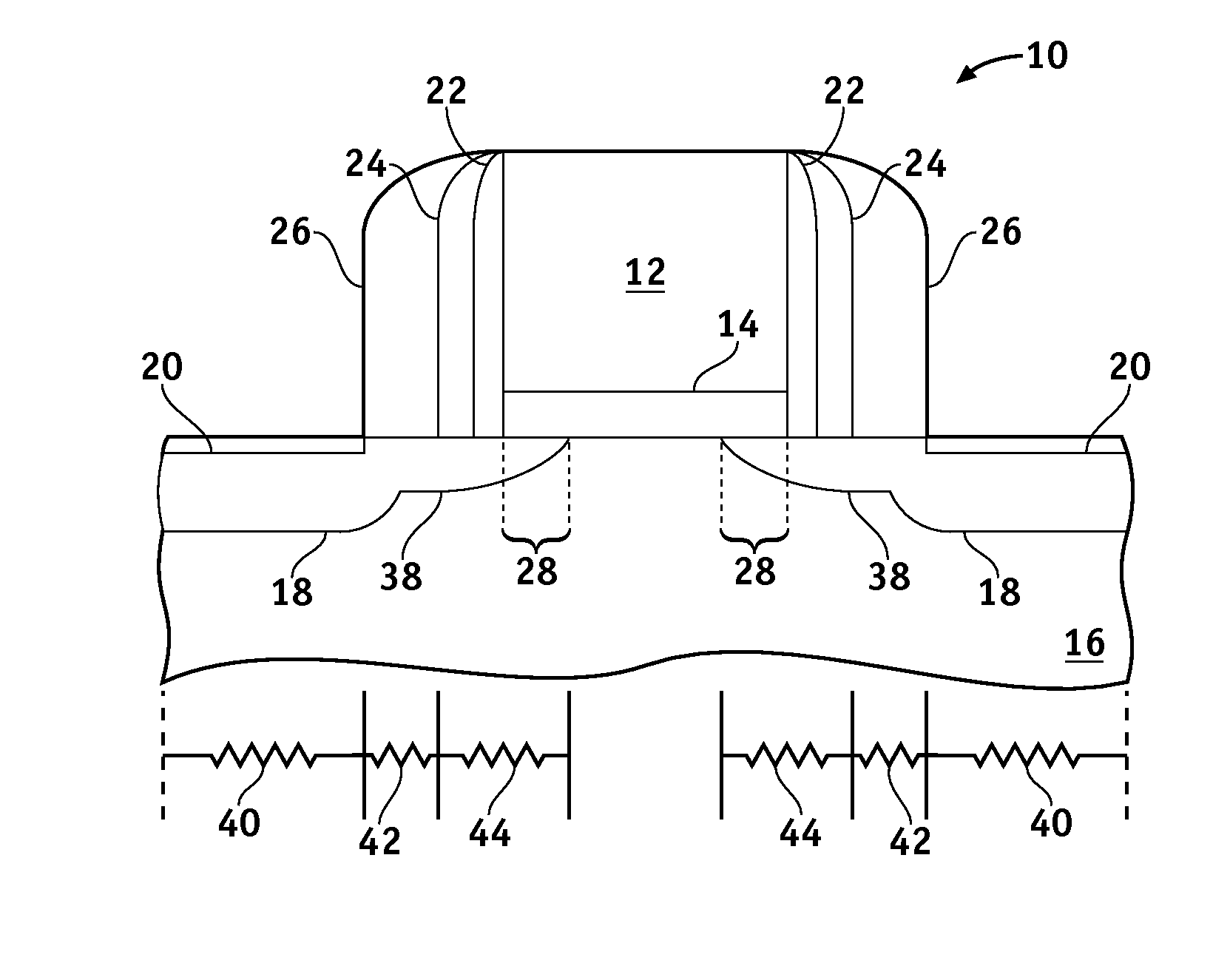
[0018]FIG. 1 schematically illustrates various components of the external resistance of a conventional MOS transistor 10. As illustrated in FIG. 1, MOS transistor 10 comprises a gate electrode 12 overlying a gate insulator 14, which are disposed on a semiconductor substrate 16. The transistor 10 also comprises shallow source and drain extensions 38 and deep source and drain regions 18 formed within the semiconductor substrate 16. Conductive contacts 20 are disposed on the source / drain regions 18. Typical with most conventional transistors, MOS transistor 10 has a reoxidation sidewall spacer 22, which is formed by subjecting the gate electrod...


PUM


Abstract

MOS transistors having high-k spacers and methods for fabricating such transistors are provided. One exemplary method comprises forming a gate stack overlying a semiconductor substrate and forming an offset spacer about sidewalls of the gate stack. The offset spacer is formed of a high-k dielectric material that results in a low interface trap density between the offset spacer and the semiconductor substrate. First ions of a conductivity-determining impurity type are implanted into the semiconductor substrate using the gate stack and the offset spacer as an implantation mask to form spaced-apart impurity-doped extensions.

Description

FIELD OF THE INVENTION[0001]The present invention generally relates to semiconductor devices and methods for fabricating semiconductor devices, and more particularly relates to MOS transistors having high-k offset spacers that reduce external resistance and methods for fabricating MOS transistors having high-k offset spacers.BACKGROUND OF THE INVENTION[0002]The majority of present day integrated circuits (ICs) are implemented by using a plurality of interconnected field effect transistors (FETs), also called metal oxide semiconductor field effect transistors (MOSFETs or MOS transistors). An MOS transistor includes a gate electrode as a control electrode that is formed on a semiconductor substrate and spaced-apart source and drain regions formed within the semiconductor substrate and between which a current can flow. A control voltage applied to the gate electrode controls the flow of current through a channel in the semiconductor substrate between the source and drain regions beneat...

Claims


Application Information

Patent Timeline
Patent Type & Authority Applications(United States)
IPC IPC(8): H01L29/94H01L21/4763
CPCH01L21/26513H01L21/28114H01L29/4983H01L29/512H01L29/665H01L29/6656H01L29/6659
Inventor HARGROVE, MICHAEL
Owner ADVANCED MICRO DEVICES INC
Why Eureka
Try Eureka