
Flip-flop and semiconductor integrated circuit

a technology of integrated circuits and flip-flops, which is applied in the direction of pulse generators, pulse techniques, electrical apparatus, etc., can solve the problems of difficult to utilize mtcmos technology in designing asics (application specific integrated circuits), and difficulty in regulating timing between control signals on the one hand, so as to facilitate timing adjustment

Inactive Publication Date: 2008-10-23
SONY CORP
View PDF3 Cites 42 Cited by
  • Summary
  • Abstract
  • Description
  • Claims
  • Application Information

AI Technical Summary

Benefits of technology

[0010]The present invention has been made in view of the above circumstances and provides arrangements for making the timing adjustments easier in partially stopping the supply of power to flip-flops.
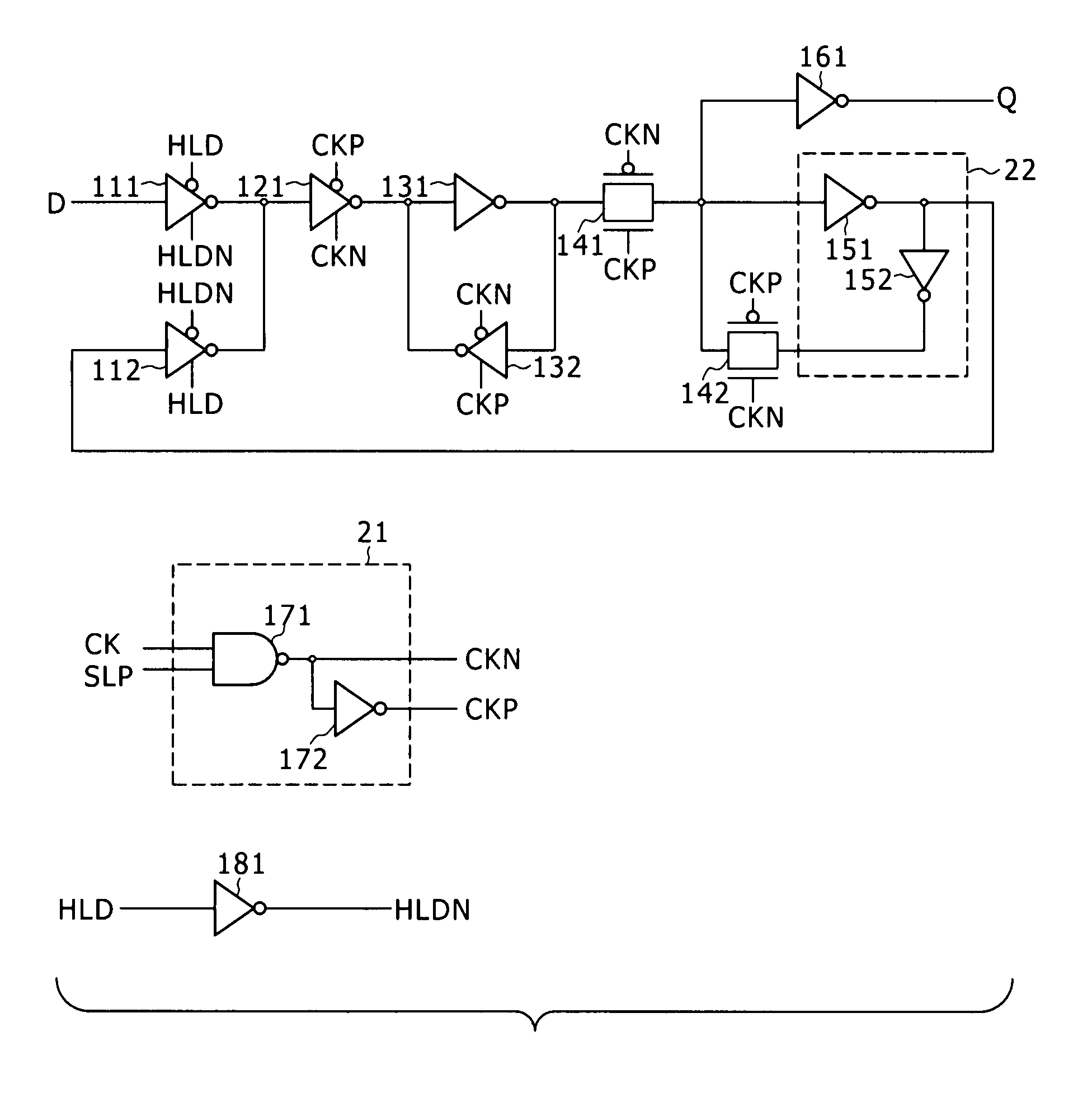
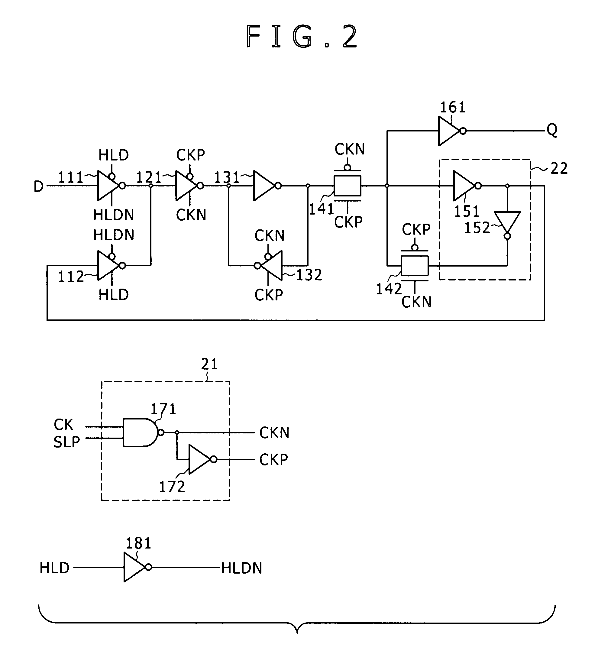
[0013]According to another embodiment of the present invention, there is provided a flip-flop including: a clock supply circuit configured to output a clock signal alternating between a first state and a second state when a sleep signal is inactive, and to fix the clock signal in the first state when the sleep signal is active; a first holding circuit configured to fetch an input signal while the clock signal is indicating the first state, and to hold the input signal while the clock signal is indicating the second state; a second holding circuit configured to fetch a first signal output by the first holding circuit while the clock signal is indicating the second state, and to hold the first signal while the clock signal is indicating the first state; an input switching circuit configured to supply as the input signal a second signal output by the second holding circuit either when a hold signal is active or when an enable signal is inactive, and to supply an external signal as the input signal both when the hold signal is inactive and when the enable signal is active; and a power supply control circuit configured to supply power to the first holding circuit and the input switching circuit when a power supply control signal is active, and not to supply power to the first holding circuit and the input switching circuit when the power supply control signal is inactive. The flip-flop according to this embodiment of the present invention allows the second holding circuit to hold the signal while the first holding circuit and input switching circuit are not being powered, and to feed the signal back to the first holding circuit when the hold signal is active or the enable signal is inactive.
[0016]The present invention, when embodied illustratively as outlined above, makes it appreciably easier to adjust the timings for stopping in part the supply of power to flip-flops.

Problems solved by technology

However, if part of each flip-flop is made up of MTCMOS elements, it is difficult to regulate the timings between control signals on the one hand, and a data input signal and a clock signal on the other hand for the MTCMOS switch.
Specifically, where the slave flip-flop is to hold data in standby mode, the master flip-flop could erroneously fetch the next data input signal when the clock signal is stopped or again activated.
The controls involved thus make it difficult to utilize the MTCMOS technology in designing ASICs (application specific integrated circuits).

Method used


Image

  • Flip-flop and semiconductor integrated circuit
  • Flip-flop and semiconductor integrated circuit
  • Flip-flop and semiconductor integrated circuit

Examples


Embodiment Construction

[0026]Preferred embodiments of the present invention will now be described in detail with reference to the accompanying drawings.

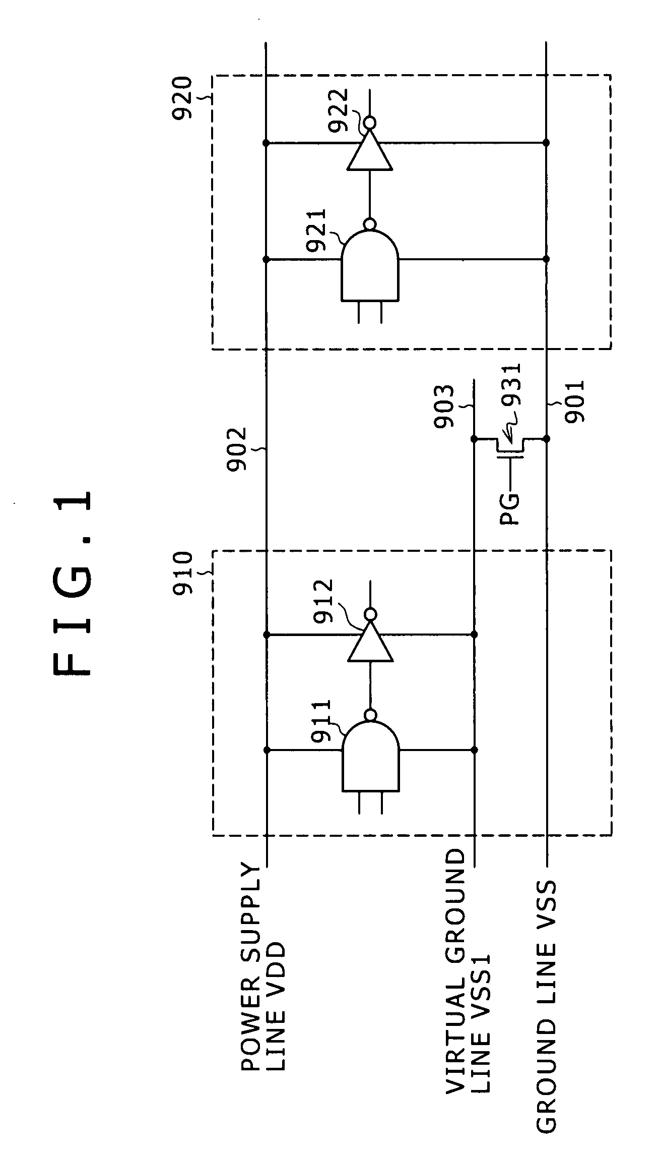
[0027]FIG. 1 is a schematic circuit diagram illustrating a basic circuit structure of an MTCMOS. In the MTCMOS, a functional block 910 has logic gates 911 and 912 connected to a virtual ground line VSS1 (903). An MTCMOS switch 931 is connected interposingly between the virtual ground line VSS1 (903) and an actual ground line VSS (901). In standby mode, the MTCMOS switch 931 is disconnected by a control signal PG, cutting off the supply of power to the MTCMOS and preventing leak currents flowing from a power supply line VDD (902) to the ground line VSS (901). Since the power supply line VDD (902) is connected to a PMOS substrate and the ground line VSS (901) to an NMOS substrate, the substrate current will not be interrupted even after the MTCMOS switch 931 is disconnected.

[0028]In a non-MTCMOS functional block 920, logic gates 921 and 922 are connected to ...


PUM


Abstract

A flip-flop is disclosed which includes: a clock supply circuit configured to output or fix a clock signal alternating between two predetermined states in accordance with a sleep signal; a first holding circuit configured to fetch or hold an input signal in accordance with a state the clock signal indicates; a second holding circuit configured to fetch or hold a first signal output by the first holding circuit in accordance with a state the clock signal indicates; an input switching circuit configured to supply as the input signal a second signal output by the second holding circuit or to supply an external signal as the input signal in accordance with the hold signal; and a power supply control circuit configured to supply or not to supply power to the first holding circuit and the input switching circuit in accordance with a power supply control signal.

Description

CROSS REFERENCES TO RELATED APPLICATIONS[0001]The present invention contains subject matter related to Japanese Patent Application JP 2006-331477 filed with the Japan Patent Office on Dec. 8, 2006, the entire contents of which being incorporated herein by reference.BACKGROUND OF THE INVENTION[0002]1. Field of the Invention[0003]The present invention relates to a semiconductor integrated circuit. More particularly, the invention relates to a semiconductor integrated circuit capable of controlling part of the power being supplied to its flip-flops.[0004]2. Description of the Related Art[0005]MTCMOS (multi-threshold-voltage complementary metal oxide semiconductor) technology has been known as a way to save power in semiconductor integrated circuits. The circuit blocks to which the MTCMOS technology is applied include functional blocks with low thresholds for operating on low voltages and switches for shutting down leak currents in a standby state.[0006]Illustratively, as shown in FIG. ...

Claims


Application Information

Patent Timeline
Patent Type & Authority Applications(United States)
IPC IPC(8): H03K3/289
CPCH03K3/356156H03K3/012H03K3/037
Inventor MOTOMURA, TETSUO
Owner SONY CORP
Learn More