Method for forming bumps on under bump metallurgy

Inactive Publication Date: 2008-10-23
ADVANCED SEMICON ENG INC
View PDF1 Cites 33 Cited by
  • Summary
  • Abstract
  • Description
  • Claims
  • Application Information

AI Technical Summary

Benefits of technology

[0013]According to the method of the present invention for forming metal bumps, the solder is applied to the metal layer by printing and the solder is reflowed to melt before the photoresist layer is removed. In this way the photoresist layer can act as a dam to prevent the molten

Problems solved by technology

Moreover, since the flow of the molten solder is limited by the photoresist layer, the sol

Method used


Image

  • Method for forming bumps on under bump metallurgy
  • Method for forming bumps on under bump metallurgy
  • Method for forming bumps on under bump metallurgy

Examples


Embodiment Construction

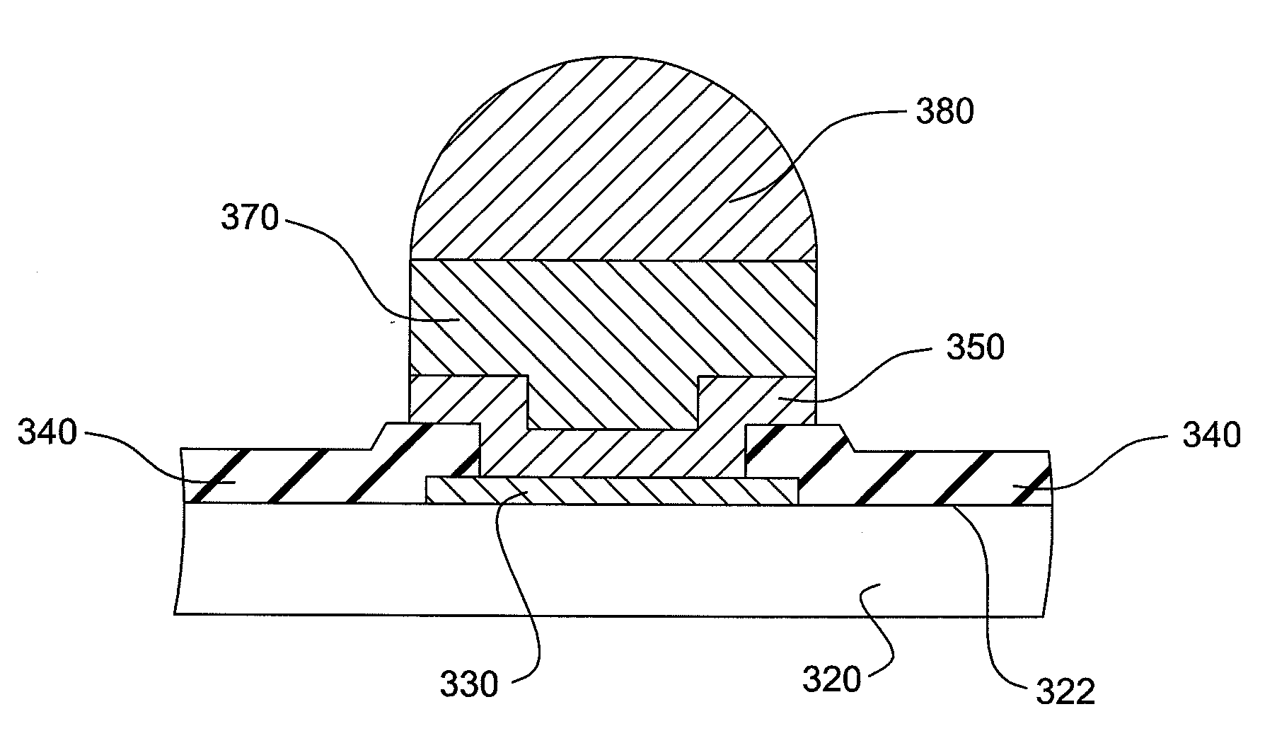
[0018]Referring to FIGS. 3a to 3g, the method for forming metal bumps according to the present invention is to form a bonding pad 330 on the active surface 322 of a chip 320 (see FIG. 3a). A passivation layer 340 is then formed on the active surface 322 of the chip 320 and exposes the bonding-pad 330 (see FIG. 3b). Afterward an under bump metallurgy 350 is formed on the active surface 322 of the chip 320 to overlay the bonding pad 330. The under bump metallurgy 350 is made of a material selected from a group consisting of titanium, alloy of titanium and tungsten, copper, nickel, alloy of chromium and copper, alloy of nickel and vanadium, alloy of nickel and gold, aluminum and combination thereof (see FIG. 3c). A layer of patterned photoresist 360 is formed on the under bump metallurgy 350 and exposes the portion of the under bump metallurgy 350 on the bonding pad 330 (see FIG. 3d). A layer of metal 370, such as copper is plated on the exposed portion of the under bump metallurgy 350...


PUM


Abstract

A method for forming metal bumps is provided. A bonding pad is first formed on the active surface of a chip and then a passivation layer is formed on the active surface of the chip and exposes the bonding pad. An under bump metallurgy is formed on the active surface of the chip to overlay the bonding pad. A layer of patterned photoresist is formed on the under bump metallurgy and exposes the portion of the under bump metallurgy on the bonding pad. A layer of copper is plated on the exposed portion of the under bump metallurgy and then a layer of solder is printed on the copper layer. Afterward the solder is reflowed to form a spherical metal bump. Finally, the photoresist layer is removed and the exposed portion of the under bump metallurgy is etched out.

Description

CROSS REFERENCE TO RELATED APPLICATION[0001]This application claims the priority benefit of Taiwan Patent Application Serial Number 096113466 filed Apr. 17, 2007, the full disclosure of which is incorporated herein by reference.BACKGROUND OF THE INVENTION[0002]1. Field of the Invention[0003]The invention relates to a method for forming bumps and more particularly, to a method for forming bumps on under bump metallurgy by printing.[0004]2. Description of the Related Art[0005]It is common that a chip is electrically connected to external circuitry by wire-bonding in the art. However, more room is required to accommodate the bonding wires and the working frequency of the chip is also limited. Therefore, to solve the above problems, the flip-chip bonding technology has been developed to replace the conventional wire-bonding technology.[0006]The so-called flip-chip bonding technology is first to form under bump metallurgy on a chip and metal bumps are then formed on the under bump metall...

Claims


Application Information

Patent Timeline
IPC IPC(8): H01L21/44
CPCH01L24/11H01L2224/1147H01L2224/13099H01L2224/16H01L2924/01013H01L2924/01022H01L2924/01029H01L2924/01074H01L2924/01078H01L2924/01079H01L2924/01005H01L2924/01006H01L2924/01023H01L2924/01024H01L2924/01033H01L2924/014H01L24/03H01L24/05H01L2224/0361H01L2224/03912H01L2224/0401H01L2224/05001H01L2224/05022H01L2224/05572H01L2224/05624H01L2224/05644H01L2224/05647H01L2224/05655H01L2224/05666H01L2224/05671H01L2224/05684H01L2224/11849H01L2924/00014H01L2924/013H01L2224/05099
Inventor CHEN, CHIEN FANHUANG, MIN LUNG
Owner ADVANCED SEMICON ENG INC
Why Eureka
Try Eureka