Differential signal layout printed circuit board

a printed circuit board and signal layout technology, applied in the direction of printed circuit aspects, cross-talk/noise/interference reduction, instruments, etc., can solve the problems of difficult application to a typical 2-layer pcb, easy bending of pcb, and inconvenient cost reduction

Active Publication Date: 2008-10-30
ASUSTEK COMPUTER INC
View PDF2 Cites 42 Cited by
  • Summary
  • Abstract
  • Description
  • Claims
  • Application Information

AI Technical Summary

Problems solved by technology

However, this is difficult to apply to a typical 2-layer PCB.
To realize this on a two layer PCB, as the signal layer 12 and the ground layer 10 need to be 4.5 mil apart, the PCB can be easily bent and it is also problematic in industrial technologies as well as not being cost effective.

Method used


Image

  • Differential signal layout printed circuit board
  • Differential signal layout printed circuit board
  • Differential signal layout printed circuit board

Examples


Embodiment Construction

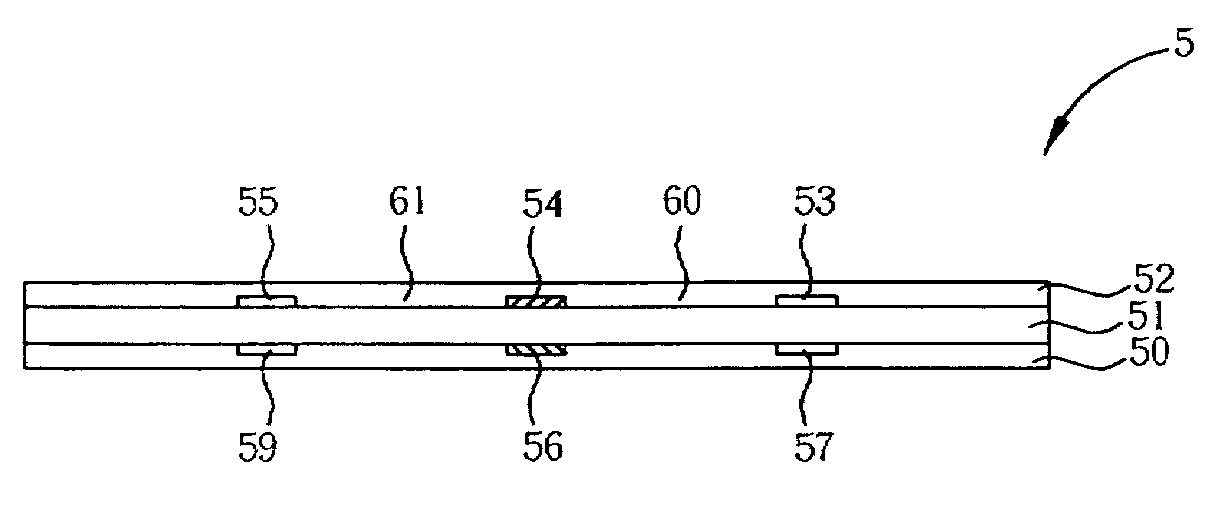
[0015]Please refer to FIG. 3. FIG. 3 is a side view of a PCB 5 in the present invention. The PCB 5 comprises an insulation layer 51, a first layer 52 and a second layer 50. The first layer 52 and the second layer 50 are disposed on two sides of the insulation layer 51. On the first layer 52 is disposed a positive differential signal trace 54 and two ground traces 53 and 55, and a space 60 between the positive differential signal trace 54 and the ground trace 53 is the same as a space 61 between the positive differential signal trace 54 and the ground trace 55. Similarly, on the second layer 50 is disposed a negative differential signal trace 56 and two ground traces 57 and 59 corresponding to the positive differential signal trace 54 and the two ground traces 53 and 55 of the first layer 52, with all traces having the same width.

[0016]Please refer to FIG. 4. FIG. 4 is a side view of another embodiment of a PCB 6 in the present invention. The PCB 6 comprises two layers 50 and 52, and...


PUM


Abstract

A positive differential signal trace and a negative differential signal trace are formed on different layers of a printed circuit board. A first ground trace is formed on the layer on which the positive differential signal trace is formed, and a second ground trace is formed on the layer on which the negative differential signal trace is formed. An insulation layer is positioned between the two layers and has a predetermined thickness. A differential mode impedance and a common mode impedance of differential signals are dependent on the predetermined thickness of the insulation layer, width and thickness of each differential signal trace, and a space between each differential signal trace and the corresponding ground trace formed on the same layer.

Description

BACKGROUND OF THE INVENTION[0001]1. Field of the Invention[0002]The present invention relates to printed circuit boards, and in particular, to a printed circuit board with a differential signal layout on different layers.[0003]2. Description of the Prior Art[0004]According to the Universal Serial Bus (USB) 2.0 specification, differential mode impedance and common mode impedance of a high speed differential signal are required to be 90 Ohms (±15%) and 30 Ohms (±30%) respectively. However, in general embodiments of edge coupling on a microstrip, a signal layer needs to be very close to a ground layer to lower impedance, and a trace width of a signal trace also varies with a space between the signal layer and the ground layer.[0005]For example, a total thickness of a four-layer Printed Circuit Board (PCB) is approximately 62 mil in general, where 40 mil is 1 mm. A first layer is the signal layer and a second layer is the ground layer with a distance between the two layers being 4.5 mil...

Claims


Application Information

Patent Timeline
Patent Type & Authority Applications(United States)
IPC IPC(8): H05K1/00
CPCG06F13/409H05K1/0219H05K1/0245H05K2201/09236H05K2201/09672
Inventor CHI, CHENG-JANKO, WEN-CHENGCHANG, SHENG-MINGTSAI, CHIH-WEI
Owner ASUSTEK COMPUTER INC
Why Eureka
Try Eureka