Low-cost and ultra-fine integrated circuit packaging technique

Active Publication Date: 2008-10-30
TAIWAN SEMICON MFG CO LTD
View PDF4 Cites 57 Cited by
  • Summary
  • Abstract
  • Description
  • Claims
  • Application Information

AI Technical Summary

Benefits of technology

[0009]In accordance with yet another aspect of the present invention, a method of forming a semiconductor package structure includes forming an interposer, which includes providing a silicon-containing substrate; forming through-silicon vias in the silicon-containing substrate; forming metal traces over the silicon-containing substrate, wherein the metal traces are connected to the through-silicon vias; and forming a first plurality of bonding pads connected to the metal traces. The method further includes providing a semiconductor chip; formin

Problems solved by technology

For example, semiconductor dies may have tightly-spaced bonding pads, which are inconvenient for being packaged onto package substrates.
However, a

Method used


Image

  • Low-cost and ultra-fine integrated circuit packaging technique
  • Low-cost and ultra-fine integrated circuit packaging technique
  • Low-cost and ultra-fine integrated circuit packaging technique

Examples


Example

[0014]The making and using of the presently preferred embodiments are discussed in detail below. It should be appreciated, however, that the present invention provides many applicable inventive concepts that can be embodied in a wide variety of specific contexts. The specific embodiments discussed are merely illustrative of specific ways to make and use the invention, and do not limit the scope of the invention.

[0015]A method for forming a semiconductor package structure having ultra-fine pitches is provided. The intermediate stages of manufacturing a preferred embodiment of the present invention are illustrated. The variations of the preferred embodiments are then discussed. Throughout the various views and illustrative embodiments of the present invention, like reference numbers are used to designate like elements.

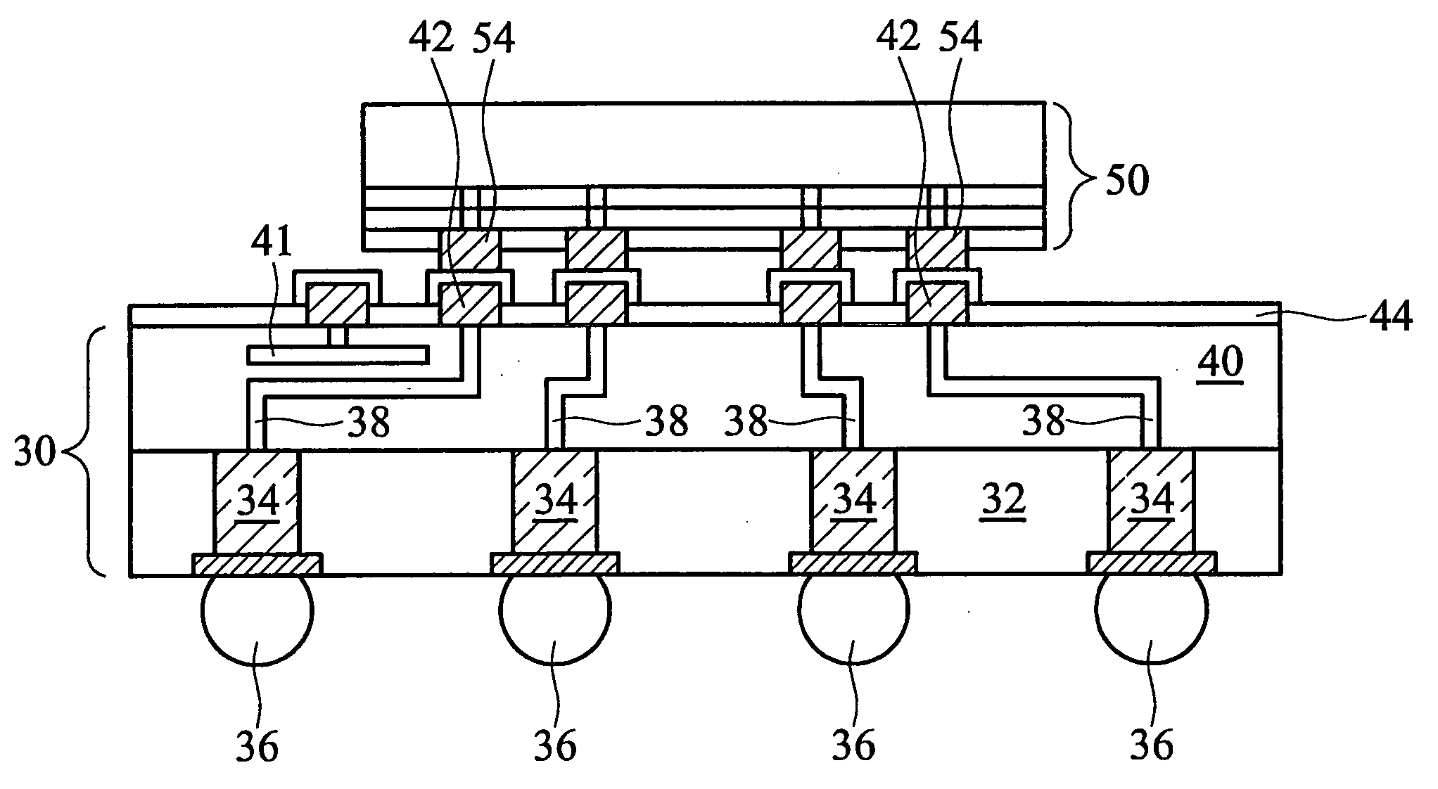
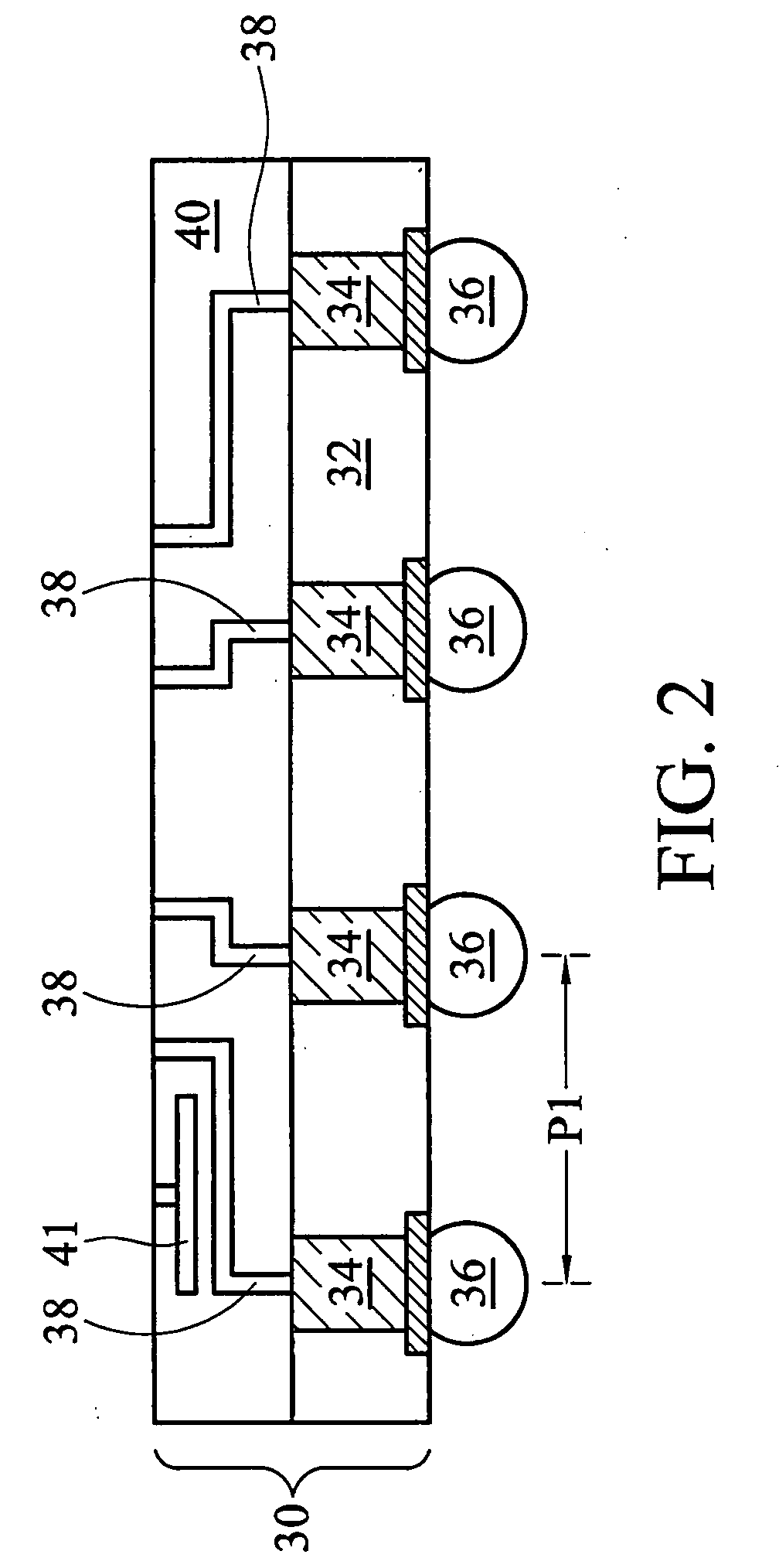
[0016]Referring to FIG. 2, interposer 30 is provided. In the preferred embodiment, interposer 30 is a silicon-containing interposer including a silicon-containing substr...


PUM


Abstract

A semiconductor package structure and the methods for forming the same are provided. The semiconductor package structure includes an interposer; a first plurality of bonding pads on a side of the interposer; a semiconductor chip; and a second plurality of bonding pads on a side of the semiconductor chip. The first and the second plurality of bonding pads are bonded through metal-to-metal bonds.

Description

TECHNICAL FIELD[0001]This invention relates generally to integrated circuit manufacturing processes, and more particularly to electronic packaging processes, and even more particularly to the bonding of dies onto interposers.BACKGROUND[0002]Interposers are used for integrated circuit packaging, typically for space transformation, which is for routing connections between semiconductor dies and packaging components. For example, semiconductor dies may have tightly-spaced bonding pads, which are inconvenient for being packaged onto package substrates. Interposers may thus be used to increase the pitches of the semiconductor dies. In this case, an interposer has a side with a first pitch, which corresponds to the pitches of the respective semiconductor dies bonded thereon. Bonding pads on the other side have a second pitch greater than the first pitch, and the second side may be bonded onto a package substrate.[0003]FIG. 1 illustrates a conventional package including interposer 10, and ...

Claims


Application Information

Patent Timeline
IPC IPC(8): H01L23/498
CPCH01L23/49816H01L23/49827H01L23/49833H01L2924/3011H01L2224/16145H01L2224/81193H01L2924/15311H01L2924/01322H01L2224/16225H01L2924/00H01L2224/05001H01L2224/056H01L24/16H01L24/13H01L2924/00014H01L2224/0557H01L2224/05009H01L2224/05568
Inventor CHAO, CLINTON
Owner TAIWAN SEMICON MFG CO LTD
Why Eureka
Try Eureka