Method of manufacturing a semiconductor device
a manufacturing method and semiconductor technology, applied in the field of manufacturing semiconductor devices, can solve the problems of ineffective electrical communication between the underlying layer and the subsequent formation of a conductive plug within the hole, and the resistance of conductive contacts (and conductive plugs) across the device,
- Summary
- Abstract
- Description
- Claims
- Application Information
AI Technical Summary
Benefits of technology
Problems solved by technology
Method used
Image

Examples
Embodiment Construction
[0024]The exemplary embodiments of the present invention are described and illustrated below to encompass methods of manufacturing semiconductor devices, as well as the resulting semiconductor devices themselves. Of course, it will be apparent to those of ordinary skill in the art that the embodiments discussed below are exemplary in nature and may be reconfigured without departing from the scope and spirit of the present invention. However, for clarity and precision, the exemplary embodiments as discussed below may include optional steps, methods, and features that one of ordinary skill should recognize as not being a requisite to fall within the scope of the present invention.
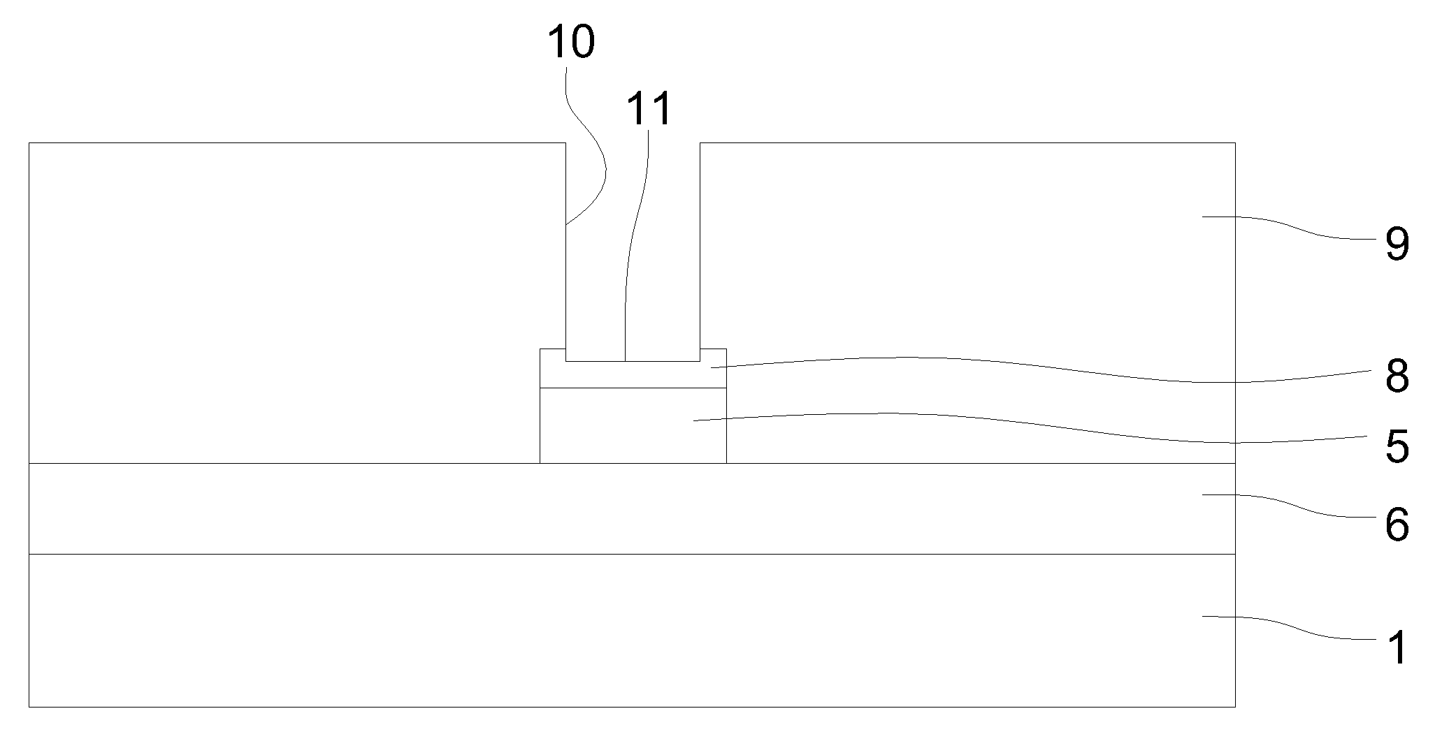
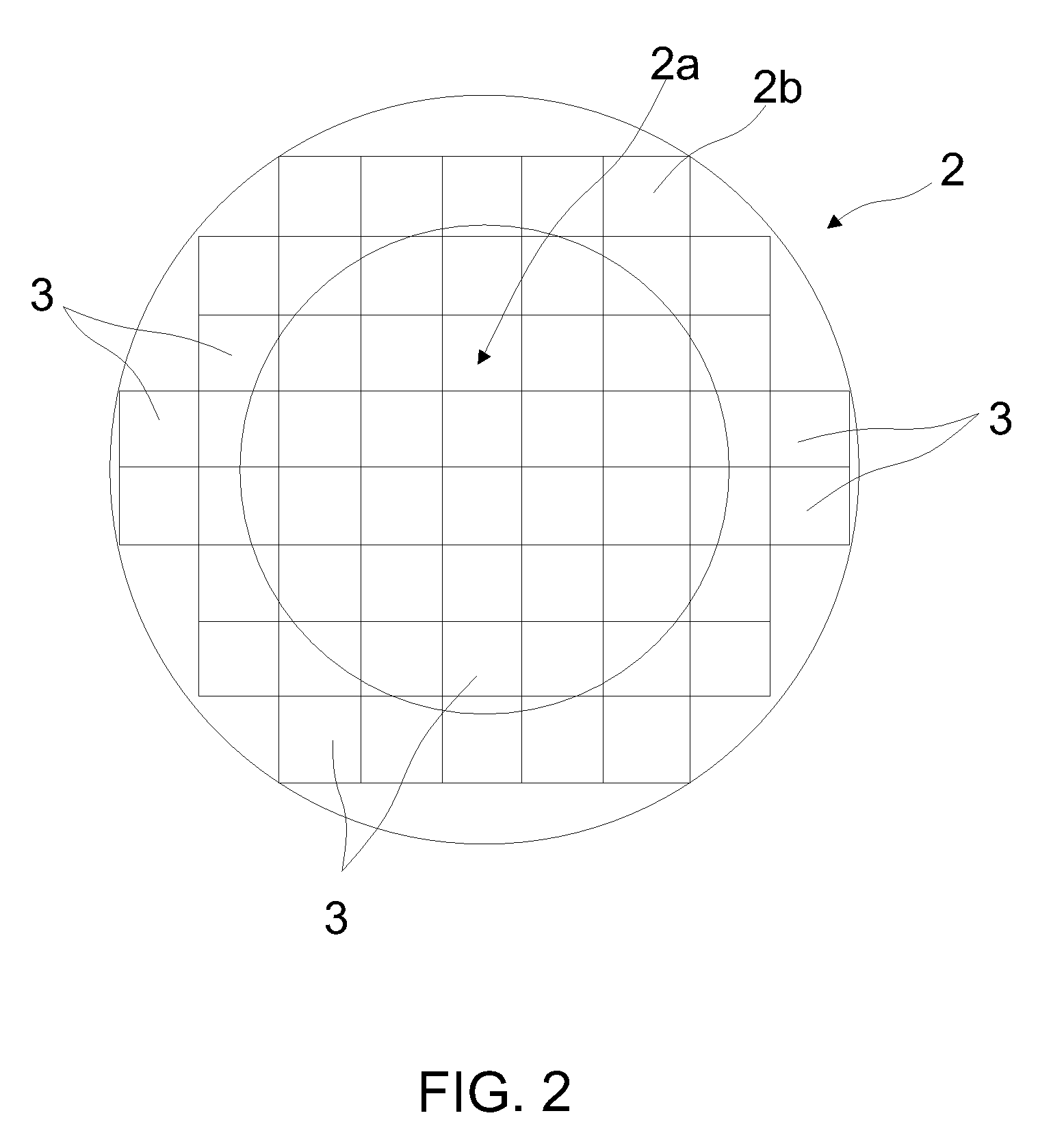
[0025]Referring to FIGS. 1 and 2, reference numeral 1 denotes a silicon semiconductor substrate of a semiconductor wafer 2. A plurality of semiconductor elements constituting a semiconductor device 3 are formed on the semiconductor substrate 1. Reference numeral 5 denotes a wiring layer that may be formed by ...
PUM
| Property | Measurement | Unit |
|---|---|---|
| temperature | aaaaa | aaaaa |
| temperature | aaaaa | aaaaa |
| pressure | aaaaa | aaaaa |
Abstract
Description
Claims
Application Information