
Test structure for semiconductor chip

a test structure and semiconductor technology, applied in the direction of semiconductor/solid-state device testing/measurement, semiconductor device details, semiconductor/solid-state device testing/measurement, etc., can solve the problem of excessive damage to surrounding materials, and achieve the effect of less damag

Inactive Publication Date: 2008-11-13
TAIWAN SEMICON MFG CO LTD
View PDF10 Cites 45 Cited by
  • Summary
  • Abstract
  • Description
  • Claims
  • Application Information

AI Technical Summary

Benefits of technology

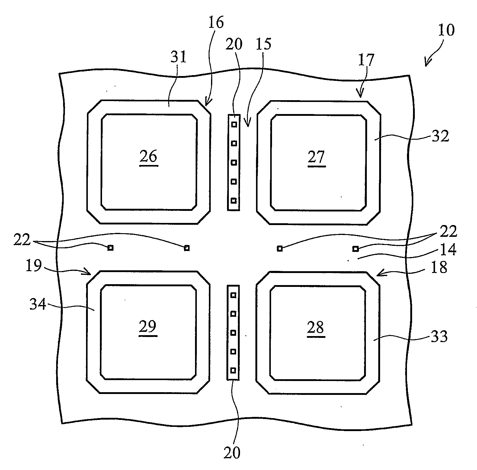
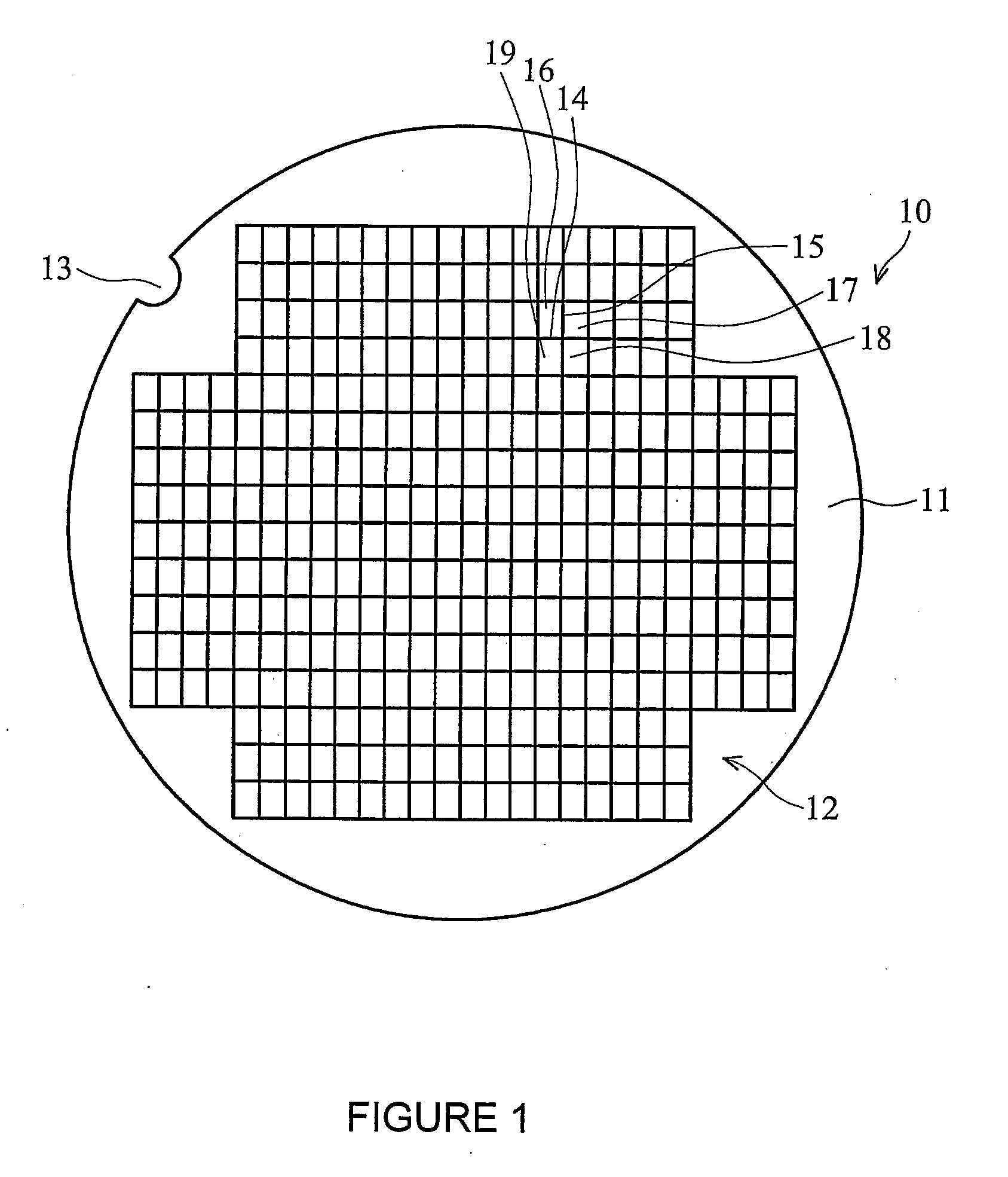
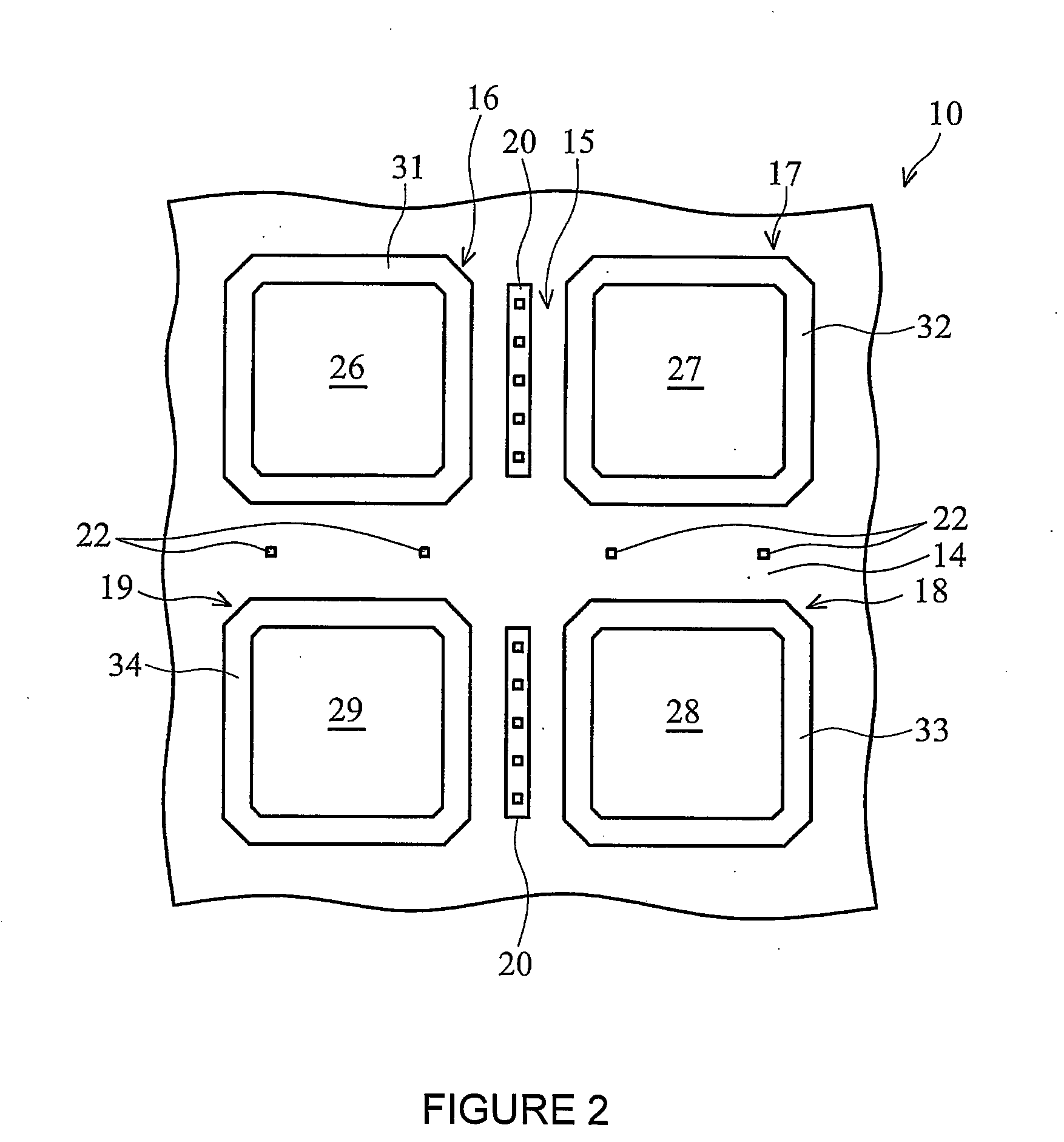
[0016]An advantage of a preferred embodiment of the present invention is that narrower scribe lines may be used between dice, and as a consequence more dice may be fabricated on the semiconductor wafer.
[0017]A further advantage of a preferred embodiment of the present invention is that by eliminating or reducing the metal materials used to make the test structures from the scribe lines, dicing may be performed by laser cutting or etching and cause less damage to the dice adjacent to the scribe line.

Problems solved by technology

In either scenario, the presence in the scribe lines of the relatively large amounts of metal associated with the PCM test structures may lead to excessive damage to surrounding materials during the sawing or dicing processes.

Method used


Image

  • Test structure for semiconductor chip
  • Test structure for semiconductor chip
  • Test structure for semiconductor chip

Examples


Embodiment Construction

[0025]The making and using of the presently preferred embodiments are discussed in detail below. It should be appreciated, however, that the present invention provides many applicable inventive concepts that can be embodied in a wide variety of specific contexts. The specific embodiments discussed are merely illustrative of specific ways to make and use the invention, and do not limit the scope of the invention.

[0026]The present invention will be described with respect to preferred embodiments in a specific context, namely a semiconductor wafer having formed upon it a number of identical dice that are separated by scribe lines, where all of the testing structures associated with the wafer and each of the dice thereon have been formed in test pattern layout areas within the active area of each die, which is surrounded by a continuous seal ring. The present invention may also be applied, however, to other semiconductor devices as well, such as those with multiple types of testing stru...


PUM


Abstract

A test structure for use in a semiconductor chip. In a preferred embodiment, a number of die are formed in an array on a semiconductor wafer substrate. Each die includes an active area defined by a seal ring and is separated from those adjacent to it by a thin scribe line. In addition to the operational structures formed in the active area of each die, one or more test structures are formed. In a preferred embodiment, these test structures are formed into one or more PCM (process control monitor) test pattern layout areas that are positioned near the seal ring and outside of the operational bond pads. Some or all of individual pads in the PCM test pattern layout area may then be connected to corresponding features on adjacent dice, and in some applications enable the simultaneous performance of WAT (wafer acceptance test) and CP (circuit probe) testing.

Description

TECHNICAL FIELD[0001]The present invention relates generally to the field of semiconductor devices, and relates more particularly to the forming of test structures on semiconductor wafers for the purpose of performing tests such as wafer acceptance test (WATs) and circuit probe (CP) tests on the wafer dice before they are separated into individual chips.BACKGROUND[0002]Semiconductor chips are small electronic devices that are used in a wide range of applications such as personal computers, cellular telephones, and gaming devices. Each chip is actually a small piece of semiconductor material onto which have been fabricated a large number of integrated circuits. Each integrated circuit, in turn, includes a number of tiny electronic components that are interconnected together. A semiconductor is a material that when properly prepared is capable of conducting electricity under certain controllable conditions, such as the application of the small electrical charge. Each of the small comp...

Claims


Application Information

Patent Timeline
IPC IPC(8): H01L23/544
CPCH01L22/34H01L23/585H01L27/0203H01L2223/5446H01L2924/0002H01L2223/54493H01L2924/00
Inventor HSU, SHIH-HSUNCHEN, HSIEN-WEIWU, ANBIARSHY N.F.
Owner TAIWAN SEMICON MFG CO LTD
Learn More