Methods for designing switchable and tunable broadband filters using finite-width conductor-backed coplanar waveguide structures

a coplanar waveguide and conductor-backed technology, applied in the field of switchable and tunable finite-width conductor-backed coplanar waveguide resonators and filters, can solve the problems of limited switchable types and tunable frequency ranges, limited frequency response, and insufficient miniaturization to meet the need for switchable and tunable filters for broadband and multi-band applications

Inactive Publication Date: 2008-11-13
NI CHI LIANG
View PDF2 Cites 14 Cited by
  • Summary
  • Abstract
  • Description
  • Claims
  • Application Information

AI Technical Summary

Benefits of technology

[0024]A further object of the invention is to provide design methods for designing broadband filters by using finite-width conductor-backed coplanar waveguide structures, which can be implemented in various structures with single layer or a plurality of layers of metallic and dielectric materials, such as those used for building integrated circuits, thin film transistors, low temperature co-fired ceramics (LTCC), high temperature co fired ceramics (HTCC), printed circuit boards (PCB), etc.

Problems solved by technology

However, miniaturization does not directly meet the need for switchable and tunable filters for both broadband and multiband applications.
Due to the fixed sizes and patterns of these configurations, the switchable types and tunable frequency range are limited.
However, there are also limitations in frequency response due to the material characterization and manufacture cost.

Method used


Image

  • Methods for designing switchable and tunable broadband filters using finite-width conductor-backed coplanar waveguide structures
  • Methods for designing switchable and tunable broadband filters using finite-width conductor-backed coplanar waveguide structures
  • Methods for designing switchable and tunable broadband filters using finite-width conductor-backed coplanar waveguide structures

Examples


Embodiment Construction

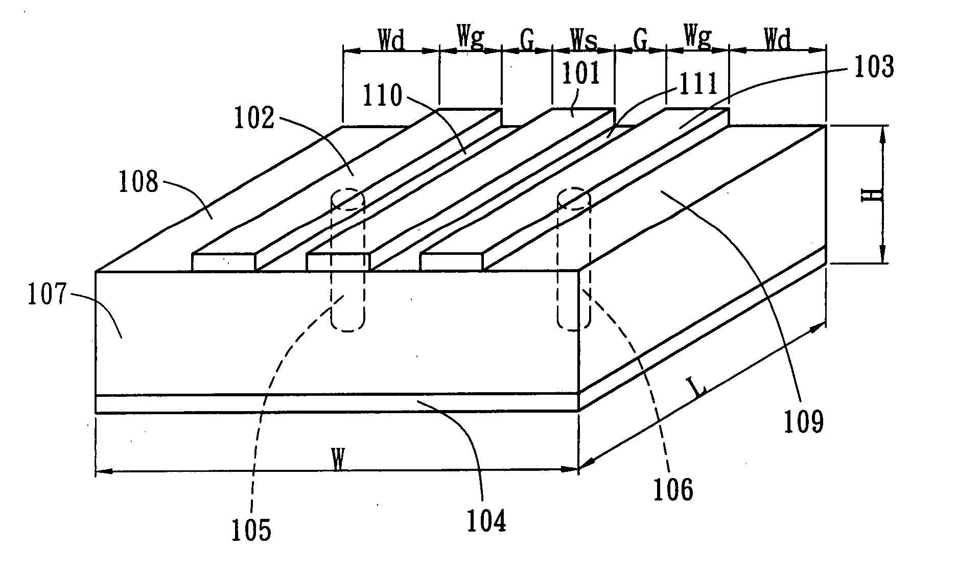
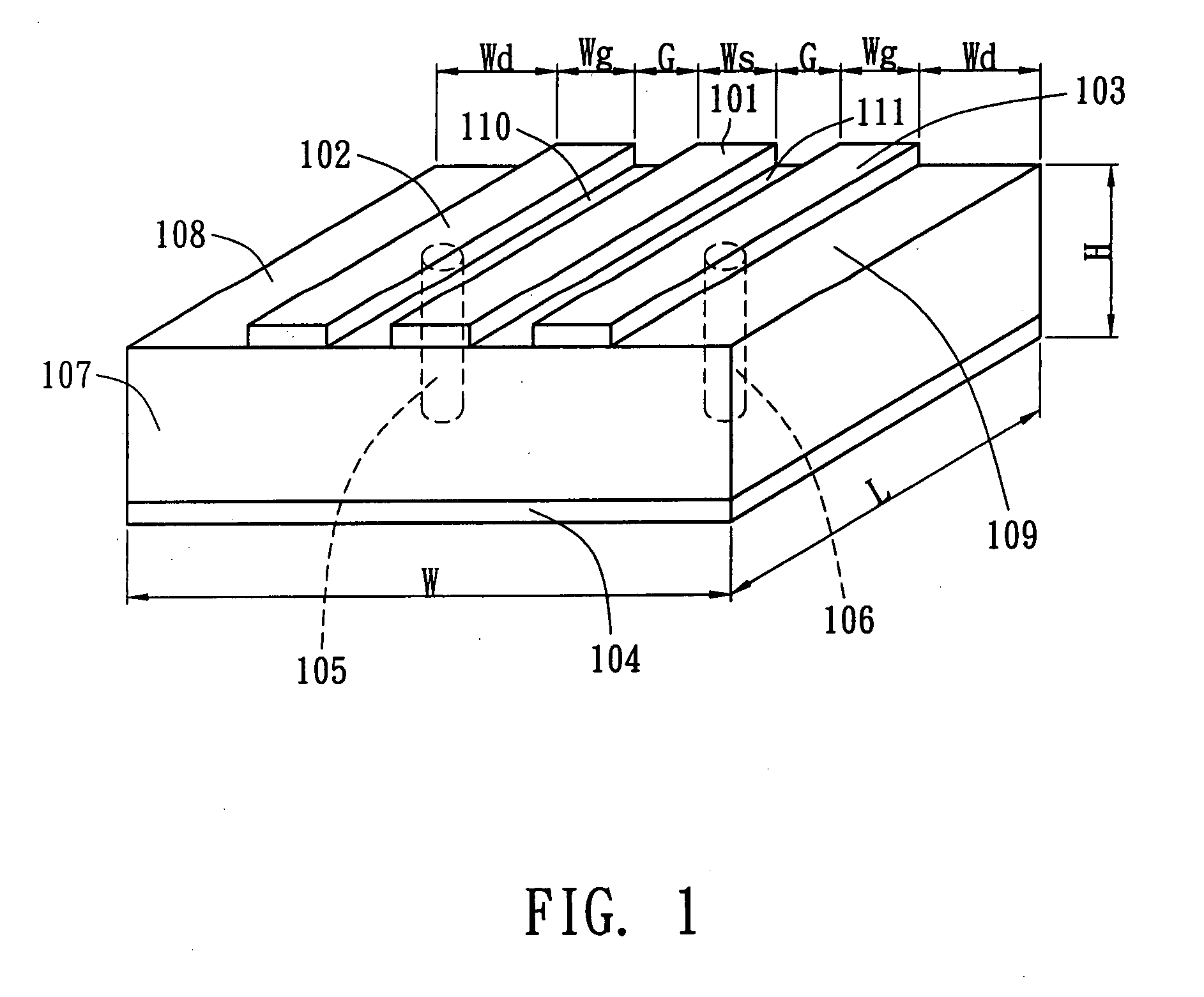
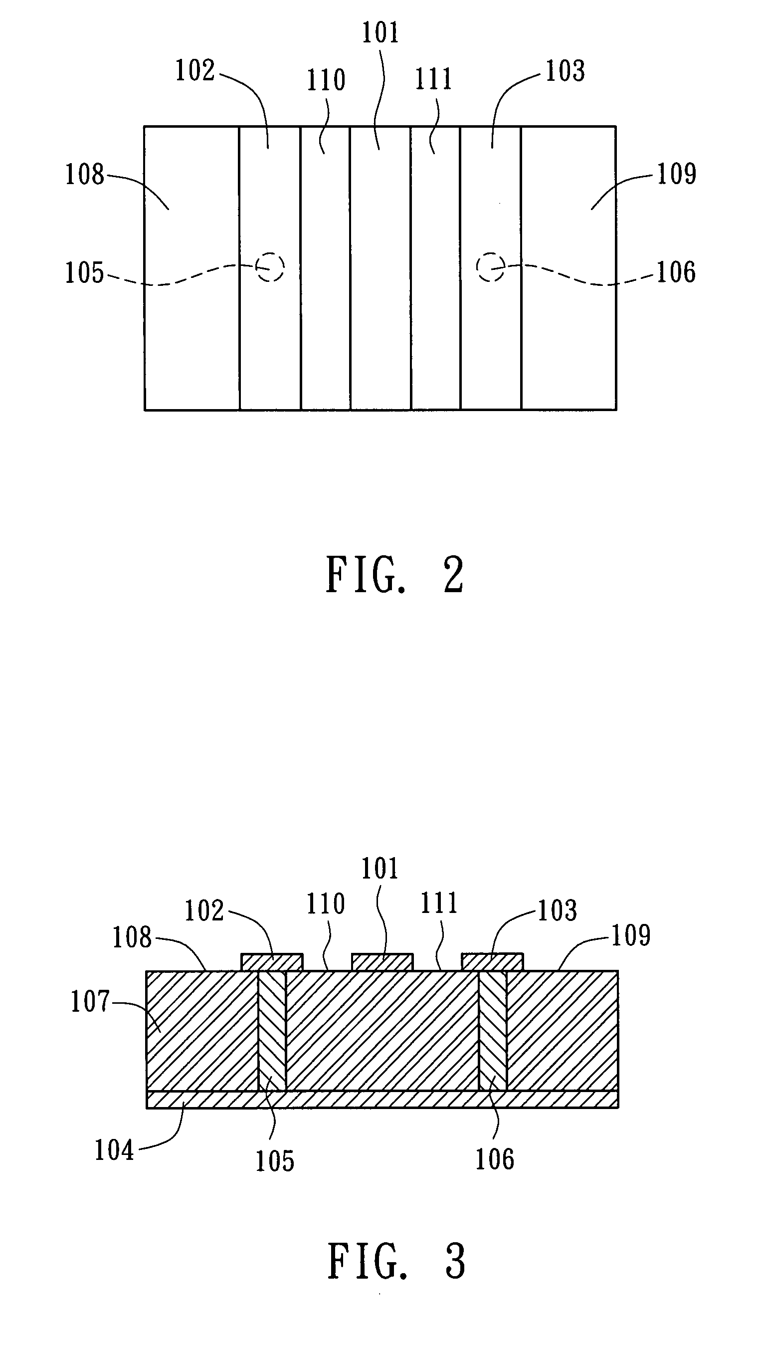
[0040]FIG. 1 illustrates a finite-width conductor-backed coplanar waveguide structures of this invention, FIG. 2 is the top view of FIG. 1; FIG. 3 is the cross sectional view of FIG. 1; herein 101 represents the metallic signal waveguide of the coplanar waveguide; 102 and 103 represent the metallic ground waveguides individually; 104 represents the metallic back conductor; 105 and 106 represent via holes including the metallic conducting posts between metallic ground waveguides 102,103 and the metallic back conductor 104; 107 represents the dielectric material; 108 and 109 represent individually the surfaces of the dielectric material without covering by metallic materials; 110 and 111 represent individually the surfaces of dielectric material 107 between metallic signal waveguide 101 and metallic ground waveguides 102 and 103; FIG. 1 shows the structures that comprising single layer dielectric material 107, and via holes including the metallic conducting posts 105 and 106, which co...


PUM


Abstract

This invention uses the structures of the finite-sized conductor-backed coplanar waveguides for designing broadband switchable and tunable signal filters. The design methods construct a plurality of configurations, which including waveguides, via holes, metallic posts, and conductor planes in the structures, for selecting, coupling, converting, and dissipating of the signals with specific electromagnetic modes and frequencies propagating through the structures. The dominant electromagnetic modes of the signals include Coplanar Waveguide Modes and Microstrip-Like Modes. The design methods thereby produce a plurality of filter types, such as bandstop filters, bandpass filters, multiband filters, etc. The design methods can apply to the structures with single and multi-layer dielectric and metallic materials, such as Integrated Circuits, Thin-film transistor Circuits, Low Temperature/High Temperature Co-fired Ceramics (LTCC/HTCC), PCB, and others. In addition, the design methods add switches to perform electrically controllable functions including frequency band selection and filter type selection. The design methods can also perform impedance matching of broadband signals by electrically tuning the values of inductance and capacitance in conjunction with the structures.

Description

TECHNICAL FIELD OF THE INVENTION[0001]This invention relates to the field of waveguides, filters, resonators and more specifically to switchable and tunable finite-width conductor-backed coplanar waveguide resonators and filters in conjunction with via holes and switches.BACKGROUND OF INVENTION[0002]The fast development of telecommunication services, such as Cellular phones, WiFi, WiMAX, RFID, Digital TV etc., faces different standards, spectrum allocations, and regulations. The portable products for these services move toward highly integrated forms as the technologies progress. To select a desirable signal or service on these products, we have been observing an increasing need exists for switchable and tunable filters for both broadband and multiband systems that are small in size, inexpensive, and easy to manufacture.[0003]Highly integrated portable telecommunication products demand system miniaturization. The design of filters evolves with the miniaturization efforts of System O...

Claims


Application Information

Patent Timeline
Patent Type & Authority Applications(United States)
IPC IPC(8): H01P1/20
CPCH01P1/2005H01P1/2013
Inventor NI, CHI-LIANG
Owner NI CHI LIANG
Why Eureka
Try Eureka