Apparatus with enhanced resolution for measuring structures on a substrate for semiconductor manufacture and use of apertures in a measuring apparatus

a technology of semiconductor manufacturing and measuring apparatus, applied in the direction of optics, measurement devices, microscopes, etc., can solve the problems that the method and r proposed here are not suitable for use in a measuring system, and achieve the effect of improving the resolution

Active Publication Date: 2008-11-13
VISTEC SEMICON SYST
View PDF6 Cites 79 Cited by
  • Summary
  • Abstract
  • Description
  • Claims
  • Application Information

AI Technical Summary

Benefits of technology

[0005]It is an object of the present invention to provide a measuring system with enhanced resolution for measuring certain periodic structures on a substrate for semiconductor manufacture.

Problems solved by technology

The method and r proposed here are not suitable for use in a measuring system which measures the position and / or the dimension of structures on a substrate.

Method used


Image

  • Apparatus with enhanced resolution for measuring structures on a substrate for semiconductor manufacture and use of apertures in a measuring apparatus
  • Apparatus with enhanced resolution for measuring structures on a substrate for semiconductor manufacture and use of apertures in a measuring apparatus
  • Apparatus with enhanced resolution for measuring structures on a substrate for semiconductor manufacture and use of apertures in a measuring apparatus

Examples


Embodiment Construction

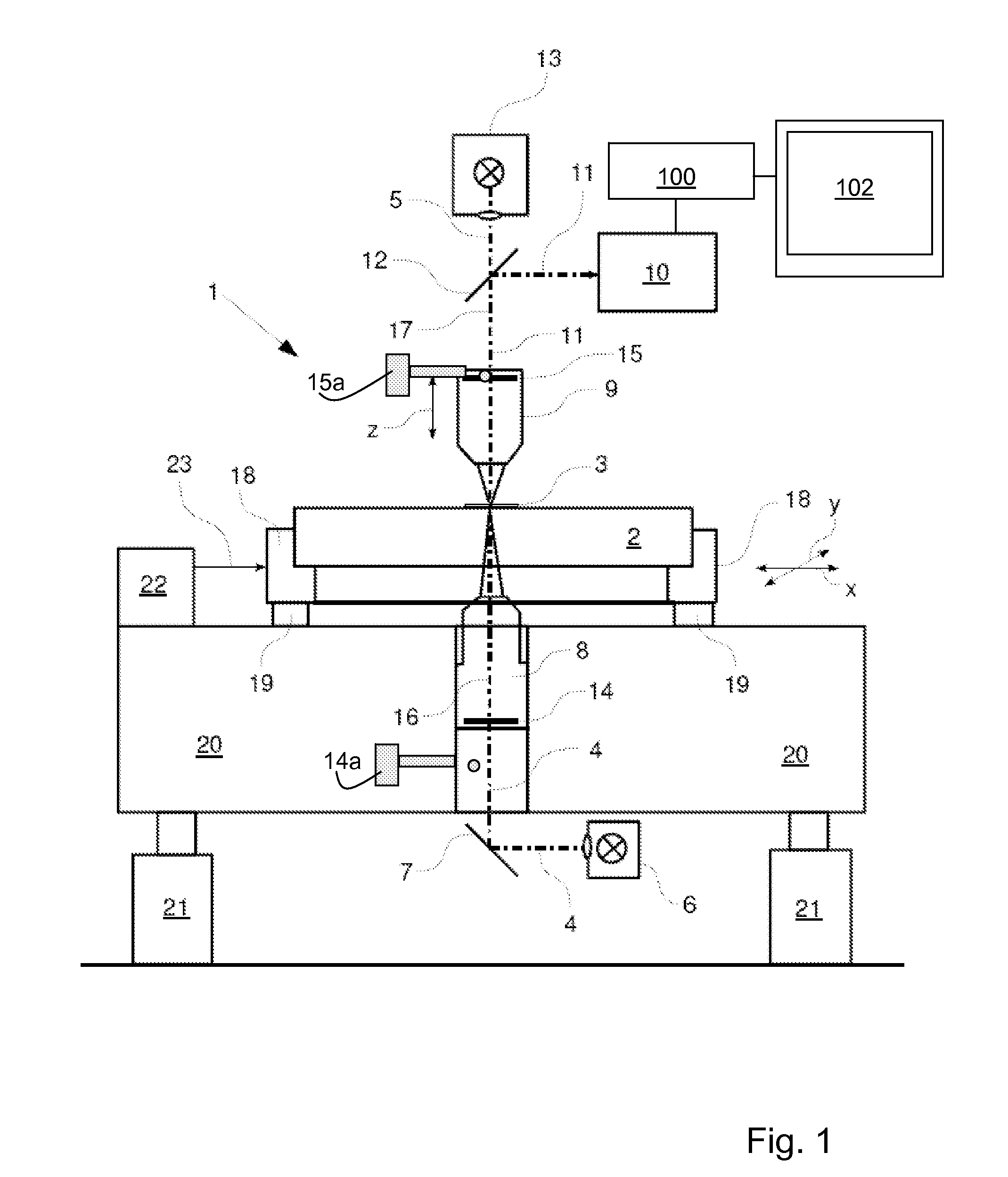
[0025]A coordinate measuring device of the type shown in FIG. 1, is an arrangement known from the state of the art, used also for measuring structures with a high measuring accuracy. The coordinate measuring device is an example of a device group used for measuring structures 3 on a substrate 2. In the case of measuring device 1, the actual measuring device itself is mounted on a vibration-damped granite block 20. The masks or wafers are placed on the measuring stage 18 by an automatic handling system. This measuring stage 18 is supported on the surface of granite block 20 by air bearings 19. Measuring stage 18 is motor driven and displaceable in two dimensions (X coordinate direction / Y coordinate direction). The corresponding driving elements are not shown. Planar mirrors are mounted on two mutually perpendicular sides of measuring stage 18. A laser interferometer system 22 is used to track the position of measuring stage 18.

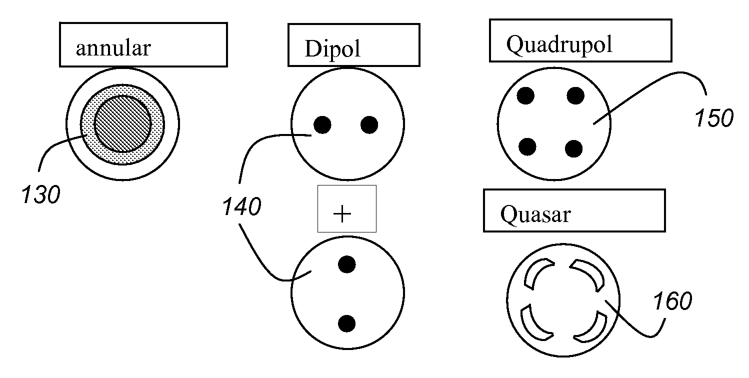
[0026]Illumination and imaging of the structures to be me...


PUM


Abstract

A measuring system is disclosed with enhanced resolution for periodic structures on a substrate for semiconductor manufacture. Aperture structures of varying geometries are provided in the illumination beam path. The aperture structures differ regarding the transmission characteristics of light, and which adjust the intensity distribution of the diffraction orders in the imaging pupil of the optical system.

Description

RELATED APPLICATIONS[0001]This application claims priority to German Patent Application No. 10 2007 021 823.2, filed on May 7, 2007, which is incorporated herein by reference in its entirety.FIELD OF THE INVENTION[0002]The present invention relates to a measuring apparatus with enhanced resolution for measuring periodic structures on a substrate for semiconductor manufacture. The measuring system comprises a condenser with an entrance pupil.[0003]The present invention further relates to the utilization of various apertures or aperture structures in the illumination beam path of a measuring system for measuring periodic structures on a substrate for semiconductor manufacture.BACKGROUND OF THE INVENTION[0004]European Patent EP 0 938 031 B1 discloses a method for the manufacture of integrated circuits using an aperture with variable transmission. Herein, an aperture comprises areas of varying transmission. The method and r proposed here are not suitable for use in a measuring system wh...

Claims


Application Information

Patent Timeline
Patent Type & Authority Applications(United States)
IPC IPC(8): G02B26/02G02B27/00
CPCG01B11/24G02B5/1857
Inventor BOESSER, HANS-ARTURSTEINBERG, WALTER
Owner VISTEC SEMICON SYST
Why Eureka
Try Eureka