Surface emitting semiconductor laser, method for fabricating surface emitting semiconductor laser, module, light source apparatus, data processing apparatus, light sending apparatus, optical spatial transmission apparatus, and optical spatial transmission system

a surface emitting semiconductor and laser technology, applied in the field of surface emitting semiconductor laser, can solve problems such as the reduction of the yield of vcsel

Active Publication Date: 2008-11-13
FUJIFILM BUSINESS INNOVATION CORP
View PDF17 Cites 42 Cited by
  • Summary
  • Abstract
  • Description
  • Claims
  • Application Information

AI Technical Summary

Problems solved by technology

Because the aperture is formed by an oxidizing reaction of Al, it is difficult to accurately control the diameter, and especially,

Method used


Image

  • Surface emitting semiconductor laser, method for fabricating surface emitting semiconductor laser, module, light source apparatus, data processing apparatus, light sending apparatus, optical spatial transmission apparatus, and optical spatial transmission system
  • Surface emitting semiconductor laser, method for fabricating surface emitting semiconductor laser, module, light source apparatus, data processing apparatus, light sending apparatus, optical spatial transmission apparatus, and optical spatial transmission system
  • Surface emitting semiconductor laser, method for fabricating surface emitting semiconductor laser, module, light source apparatus, data processing apparatus, light sending apparatus, optical spatial transmission apparatus, and optical spatial transmission system

Examples


Embodiment Construction

[0027]Referring to the accompanying drawings, exemplary embodiments for implementing the present invention will be now described.

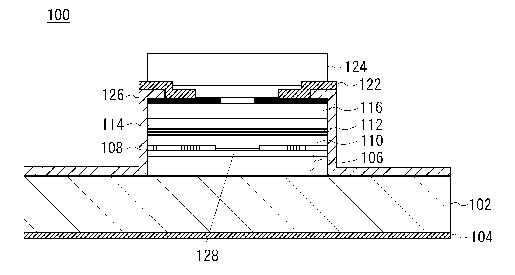
[0028]FIG. 1A and FIG. 1B are schematic cross sectional views illustrating a configuration of a VCSEL according to an example of the present invention. A VCSEL 100 according to an example includes a p-side electrode 104 on a back surface of a p-type GaAs substrate 102. Stacked on the substrate 102 are: a lower DBR (Distributed Bragg Reflector) 106 that composes a reflective mirror of multilayer films in which two types of p-type AlxGa1-xAs having different x values are overlaid one another; a current confining layer 108 made of p-type Al0.98Ga0.02As; a p-type lower spacer layer 110; an active layer 112 having a quantum well structure; an n-type upper spacer layer 114; an intermediate DBR 116 that composes a partial reflective mirror of multilayer films in which a few periods of two types of n-type AlxGa1-xAs having different x values are overlaid; an optic...


PUM


Abstract

A surface emitting semiconductor laser includes a substrate, a lower reflective mirror formed on the substrate, an active layer formed on the lower reflective mirror, an upper reflective mirror formed on the active layer, an optical mode controlling layer formed between the lower reflective mirror and the upper reflective mirror, and a current confining layer formed between the lower reflective mirror and the upper reflective mirror. The active layer emits light. The upper reflective mirror forms a resonator between the lower reflective mirror and the upper reflective mirror. In the optical mode controlling layer, an opening is formed for selectively absorbing or reflecting off light that is emitted in the active layer. The optical mode controlling layer optically controls mode of laser light. The current confining layer confines current that is applied during driving.

Description

CROSS-REFERENCE TO RELATED APPLICATIONS[0001]This application is based on and claims priority under 35 USC 119 from Japanese Patent Application No. 2007-126571 filed May 11, 2007.BACKGROUND[0002]1. Technical Field[0003]This invention relates to a surface emitting semiconductor laser, a method for fabricating a surface emitting semiconductor laser, a module, a light source apparatus, a data processing apparatus, a light sending apparatus, an optical spatial transmission apparatus, and an optical spatial transmission system.[0004]2. Related Art[0005]In technical fields such as optical communication or optical storage, there has been a growing interest in surface emitting semiconductor lasers, i.e., Vertical-Cavity Surface-Emitting Lasers (hereinafter referred to as VCSELs). VCSELs have excellent characteristics which edge-emitting semiconductor lasers do not have. For example, VCSELs feature lower threshold current and smaller power consumption. With VCSELs, a round light spot can be ...

Claims


Application Information

Patent Timeline
IPC IPC(8): H01S5/065H01L33/00H01S5/183
CPCH01S5/02284H01S5/02288H01S5/18311H01S5/18325H01S5/18327H01S5/1833H01S5/18341H01S5/18355H01S5/18369H01S5/18397H01S2301/18H01S5/02253H01S5/02251
Inventor SUZUKI, TEIICHINAGAO, DAISUKI
Owner FUJIFILM BUSINESS INNOVATION CORP
Why Eureka
Try Eureka