Method for forming a pn diode and method of manufacturing phase change memory device using the same

Inactive Publication Date: 2008-11-13
SK HYNIX INC
View PDF3 Cites 17 Cited by
  • Summary
  • Abstract
  • Description
  • Claims
  • Application Information

AI Technical Summary

Benefits of technology

[0014]Embodiments of the present invention are directed to a

Problems solved by technology

However, DRAM must have a high charge storing capacity requiring the surface area of an electrode to be increased making it difficult to accomplish a high level of integration.
It is therefore difficult to accomplish a high level of integration since a separate booster circuit is needed to form a voltage necessary for write and delete operations.
However, in the conventional phase ch

Method used


Image

  • Method for forming a pn diode and method of manufacturing phase change memory device using the same
  • Method for forming a pn diode and method of manufacturing phase change memory device using the same
  • Method for forming a pn diode and method of manufacturing phase change memory device using the same

Examples


Example

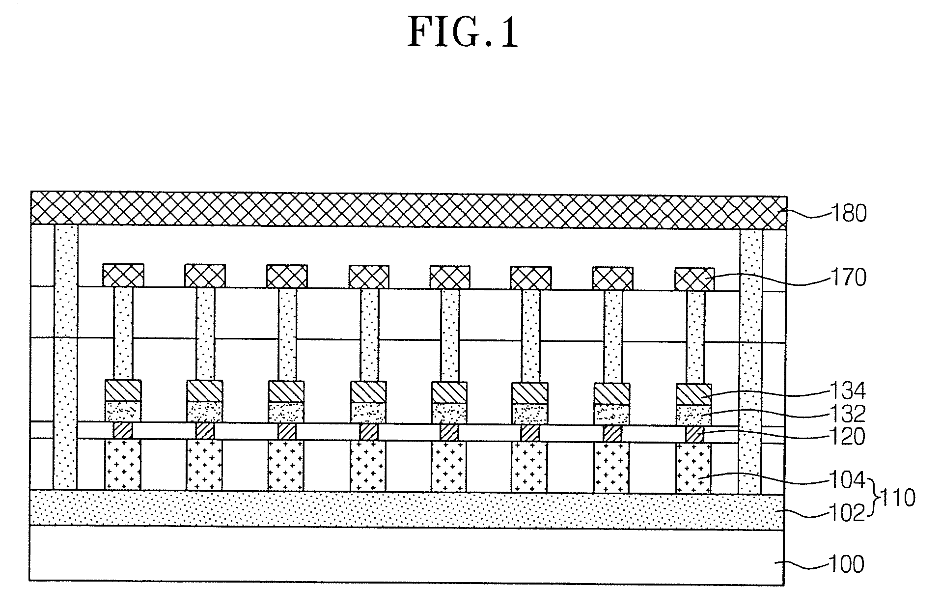
[0034]In the present invention, P-regions are formed by sequentially conducting processes for depositing a polysilicon layer doped with P-type impurities on a semiconductor substrate and etching the polysilicon layer forming a PN diode.

[0035]Therefore, in the present invention, by forming the P-regions through deposition and etching of the P-type polysilicon layer, the non-uniformity of resistance in the P-regions can be decreased as compared to the use of the SEG process in the conventional art. Accordingly, in the present invention, the characteristics of the PN diode are improved since the P-regions are stably formed. Therefore, it is possible to realize a phase change memory device having stable characteristics.

[0036]Hereafter, specific embodiments of the present invention will be described with reference to the attached drawings.

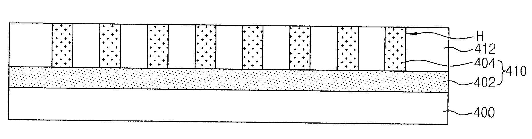
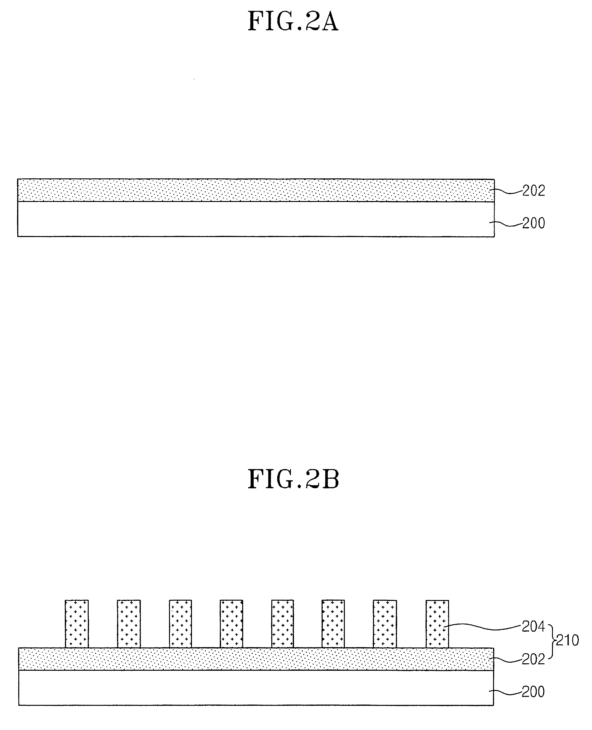
[0037]FIGS. 2A and 2B are cross-sectional views illustrating the processes for a method of forming a PN diode in accordance with an embodiment of the p...


PUM


Abstract

Disclosed is a method of forming a PN diode and a method of manufacturing a phase change memory device using the same. Formation of a PN diode includes forming a first conductivity type region in a surface of a semiconductor substrate. A polysilicon layer doped with second conductivity type impurities is then deposited on the semiconductor substrate formed with the first conductivity type region. Forming a plurality of second conductivity type regions by etching the polysilicon layer doped with the second conductivity type impurities completes the PN diode. Since the P-regions of a PN diode are formed through the deposition and etching of a polysilicon layer doped with second conductivity type impurities rather than an SEG process, a uniformity of resistance in the PN diode can be obtained.

Description

CROSS-REFERENCE TO RELATED APPLICATIONS[0001]The present application claims priority to Korean patent application number 10-2007-0046133 filed on May 11, 2007, which is incorporated herein by reference in its entirety.BACKGROUND OF THE INVENTION[0002]The present invention relates to a method of manufacturing a phase change memory device, and more particularly, to a method of forming a PN diode capable of forming stable P-regions and a method of manufacturing a phase change memory device using the same.[0003]In general, memory devices are largely divided between volatile RAM (random access memory), which loses inputted information when power is interrupted, and non-volatile ROM (read-only memory), which can continuously maintain the stored state of inputted information even when power is interrupted. Examples of volatile RAM include DRAM (dynamic RAM) and SRAM (static RAM). An example of non-volatile ROM includes flash memory such as an EEPROM (electrically erasable and programmable ...

Claims


Application Information

Patent Timeline
IPC IPC(8): H01L21/441
CPCH01L27/2409H01L29/66136H01L45/06H01L45/1233H01L45/126H01L45/144H01L45/1675H10B63/20H10N70/231H10N70/8413H10N70/826H10N70/8828H10N70/063G11C13/0004
Inventor CHANG, HEON YONG
Owner SK HYNIX INC
Why Eureka
Try Eureka