

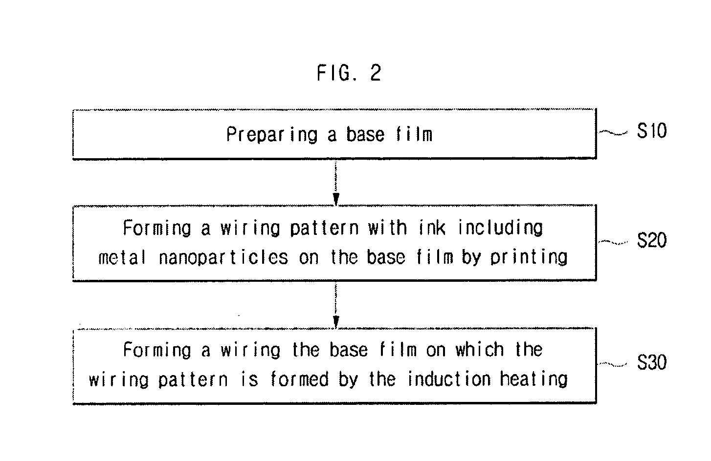
Wiring forming method of printed circuit board
a technology of printed circuit board and wiring, which is applied in the direction of printed circuits, electrical devices, printed circuit aspects, etc., can solve the problems of serious environmental problems, waste water, and energy consumption of furnaces, and the conventional methods of manufacturing products using lithography and ething cannot meet, so as to shorten the manufacturing process, improve the mechanical strength, and reduce the thermal strain of a base film
- Summary
- Abstract
- Description
- Claims
- Application Information
AI Technical Summary
Benefits of technology
Problems solved by technology
Method used
Image

Examples
example 1
[0063]Adhesion strength between a base film and a metal wiring is determined and a picture of the base film and the metal wiring is taken with a scanning electron microscope (SEM) to provide the effect of the induction heating to the adhesion between a base film and a metal wiring and the shape of the base film and the metal wiring after the adhesion test is performed.
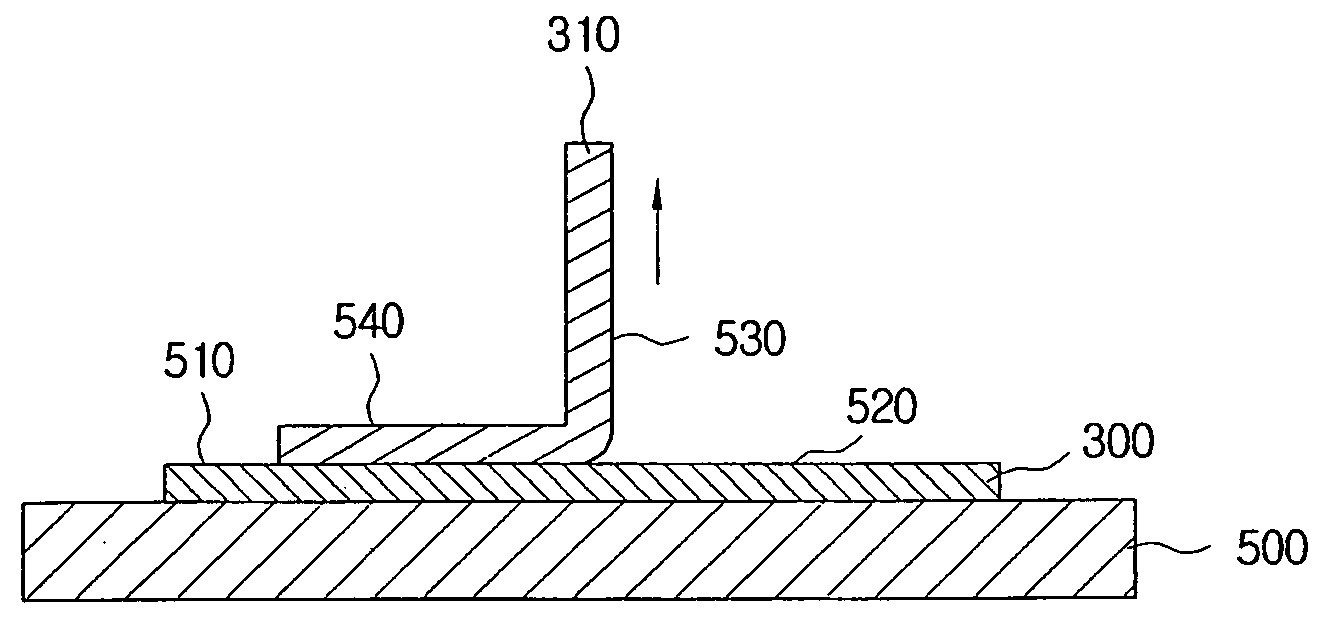
[0064]As shown in FIG. 3, a copper wiring pattern 310 having 1 cm×10 cm×10 μm of width (a)×length (b)×thickness (c) was printed on the bismaleimide triazine resin film (BT film) 300 with ink including copper nanoparticles having an average size of 20 nm by the ink-jet method.
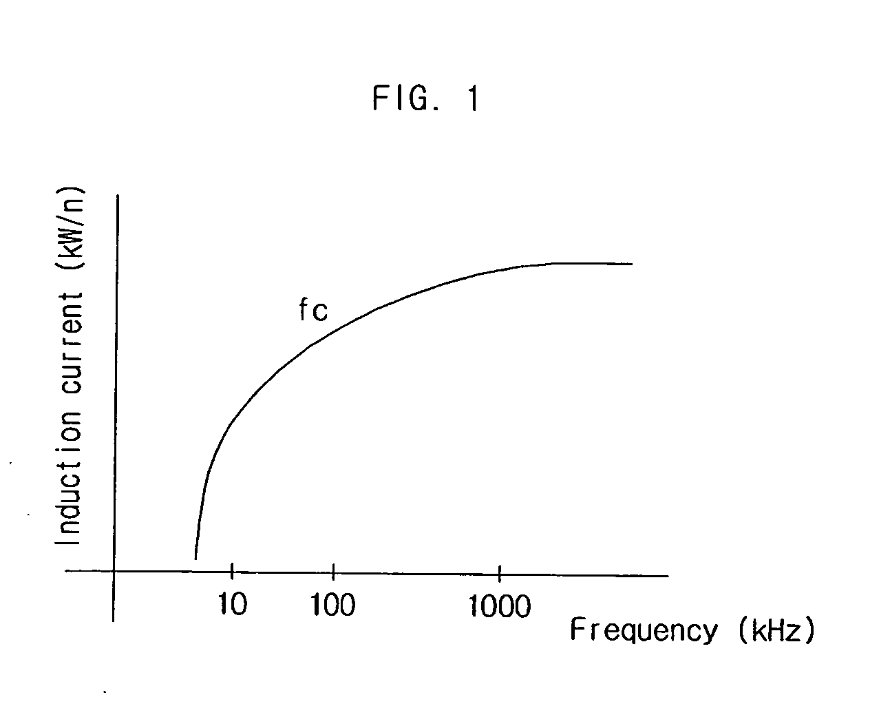
[0065]As shown in FIG. 4, after drying the copper wiring pattern 310 formed on the base film, a induction heating furnace 430 connected with a high frequency oscillator 410 was passed at an operation frequency of 500 kHz by using a conveyor belt 420. Nitrogen, argon, oxygen, hydrogen, air, organic acid gas or alcohol gas, etc. may be injected to th...
example 2
[0067]As shown in FIG. 3, a copper wiring pattern 310 having 1 cm×10 cm×10 μm of width×length×thickness was printed on the bismaleimide triazine resin film (BT film) 300 with ink including copper nanoparticles having an average size of 5 nm by the ink-jet method.
[0068]Since the copper nanoparticles having an average size of 5 nm contained 15 to 20 wt. % of an organic compound, the heat treatment at a low temperature was necessary before the induction heating to reduce the content of the organic compound. Thus, after the heat treatment at 180° C. and the drying process of the copper wiring pattern 310 which was formed on the base film, a induction heating furnace 430 connected with a high frequency oscillator 410 was passed at an operation frequency of 500 kHz by using a conveyor belt 420 as shown in FIG. 4.
[0069]In this Example, the probe microphone type heating part was used for the induction heating of the small portion including the copper wiring pattern of the printed circuit bo...
PUM
| Property | Measurement | Unit |
|---|---|---|
| Temperature | aaaaa | aaaaa |
| Diameter | aaaaa | aaaaa |
| Width | aaaaa | aaaaa |
Abstract
Description
Claims
Application Information