Method for Producing Patterned Structures by Printing a Surfactant Resist on a Substrate for Electrodeposition

a technology of surfactant resist and substrate, applied in the field of lithography, can solve the problems of inability to use in conjunction with sputter deposition or evaporation, inability to deposit material from the vapor phase, and inability to produce patterned structures. the effect of high energy, low cost and considerable cos

Inactive Publication Date: 2008-11-20
THE JOHN HOPKINS UNIV SCHOOL OF MEDICINE
View PDF6 Cites 17 Cited by
  • Summary
  • Abstract
  • Description
  • Claims
  • Application Information

AI Technical Summary

Benefits of technology

[0010]The method has several advantages over conventional methods for producing patterned materials on substrates. First, methods such as photolithography or electron-beam lithography are considerably more costly and time consuming. Second, electrodeposition has many advantages over other deposition methods. It is low cost and can be used to deposit a wide range of materials. Furthermore, electrodeposition is one of the only methods for depositing materials in a pattern formed...

Problems solved by technology

First, methods such as photolithography or electron-beam lithography are considerably more costly and time consuming.
Other methods that deposit material from the vapor phase, such as sputter deposition or...

Method used


Image

  • Method for Producing Patterned Structures by Printing a Surfactant Resist on a Substrate for Electrodeposition
  • Method for Producing Patterned Structures by Printing a Surfactant Resist on a Substrate for Electrodeposition
  • Method for Producing Patterned Structures by Printing a Surfactant Resist on a Substrate for Electrodeposition

Examples


example 1

Electrodeposition of Conductive Material

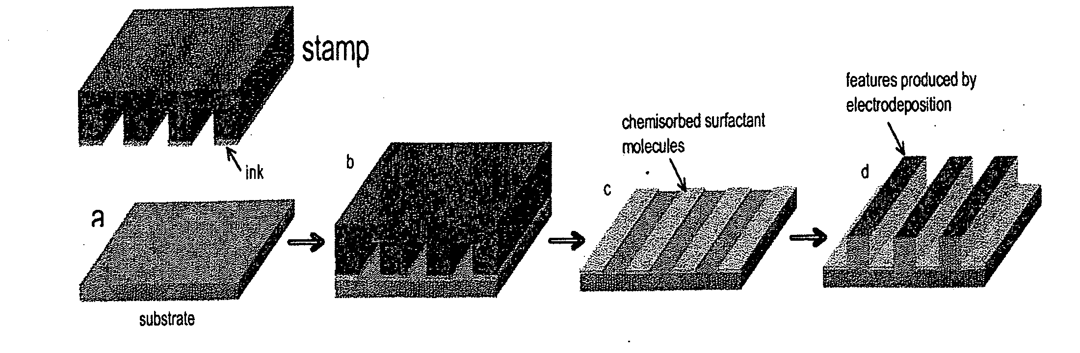
[0030]In a preferred embodiment, a molecule with a sulfhydryl group at one end is used as the surfactant molecule. A stamp is used to transfer a pattern of the surfactant molecule to a gold or silver substrate. The patterned surfactant may be used to direct deposition of a material to the surfactant-free regions. The material is deposited at a potential positive to the reduction potential for the chemisorbed surfactant molecule, that is, at a potential positive to the potential where the surfactant molecule is desorbed from the substrate. In certain embodiments of the present invention, the deposited material is not applied to the regions where the substrate is covered with the surfactant molecule. The conditions under which deposition only occurs in the surfactant-free regions of the substrate and where the material is deposited with no lateral growth to heights greater than the height of the surfactant layer are dependent on the molecular st...

example 2

Sequential Stamping

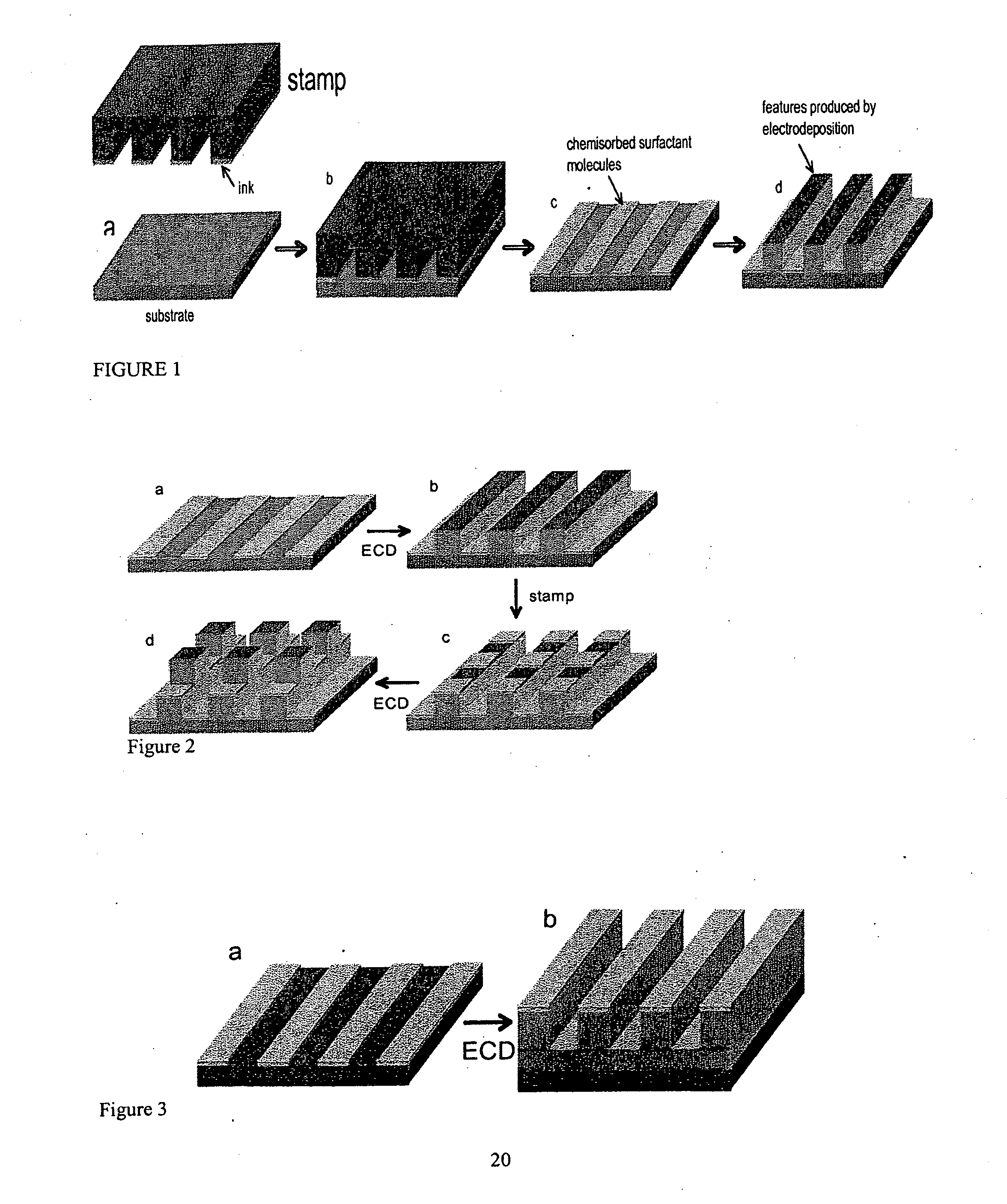
[0031]As shown in FIG. 2a, a substrate 230 is stamped with a surfactant material 220, using a stamp coated or inked with surfactant molecules, thereby transferring surfactant molecules that chemisorb onto the substrate 230 in regions where the stamp contacts the surface of the substrate 230. A conductive material 240 is deposited by electrodeposition onto the substrate to create features that grow vertically from the substrate with lateral dimensions defined by the pattern, as shown in FIG. 2b. Thereafter, the deposited material 240 obtained via the initial electrodeposition is stamped with a second layer of surfactant 250 that chemisorbs to that material.

[0032]The stamp orientation and pattern are selected to place the surfactant molecules in a pattern of interest on top of the layer of deposited material 240. On removing the stamp (FIG. 2c) the surfactant molecule is transferred to and chemisorbs only in regions where the stamp is in contact with top of the feat...

example 3

Preferential Deposition in the Regions where a Surfactant Molecule is Chemisorbed to the Surface

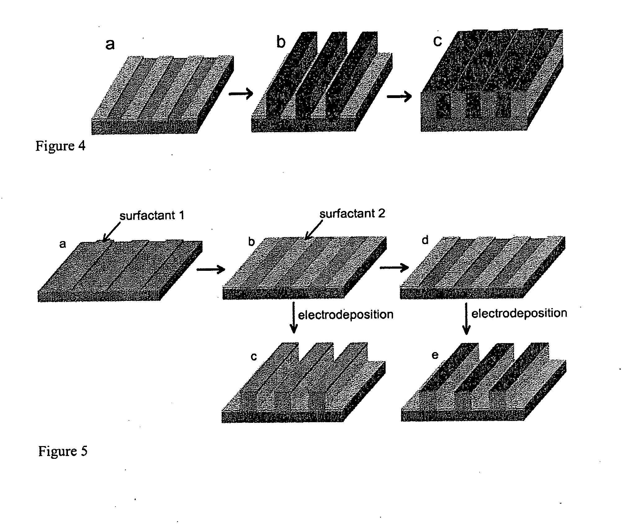
[0034]According to the embodiment depicted in FIG. 3, a substrate 330 is stamped with a surfactant material 320, using, for example, a stamp coated or inked with surfactant molecules, thereby causing the surfactant molecules 320 to chemisorb onto the substrate 330 in regions where the stamp made contact with the surface of the substrate 330, as shown in FIG. 3a. Next, a conductive material 340 is deposited by electrodeposition onto the substrate, as shown in FIG. 3b. In this embodiment, the material of interest is deposited on both the regions of the surface covered with surfactant molecules and on the regions that are not covered with surfactant molecules. The rate of deposition in the regions covered by the surfactant molecules is faster or higher than the rate of deposition in the surfactant-free regions. As shown in FIG. 3b, this preferential deposition results in the deposited featur...


PUM

PropertyMeasurementUnit
Electrical conductoraaaaaaaaaa
Areaaaaaaaaaaa
Deposition rateaaaaaaaaaa

Abstract

Methods for electrodeposition of conductive material on a conductive substrate that contains a pattern of a chemisorbed surfactant formed by a stamp having a patterned surface which is pressed onto the surface of the substrate for printing the substrate. Electrodeposition occurs by immersing the patterned substrate in a plating bath upon application of deposition potential or current to the conductive substrate. In embodiment, the chemisorbed surfactant on the surface of the substrate acts as a positive resist so that electrodeposition occurs on regions of the substrate not covered with surfactant. In another embodiment, electrodeposition occurs preferentially in regions of the substrate covered with the chemisorbed surfactant.

Description

RELATED APPLICATIONS[0001]This application is a continuation-in-part of U.S. application Ser. No. 11 / 638,137, filed Dec. 13, 2006, which is a divisional of U.S. application Ser. No. 10 / 836,021, filed Apr. 29, 2004, now abandoned, which claims priority to U.S. Provisional Application Nos. 60 / 523,498, filed Nov. 19, 2003 and 60 / 467,248, filed May 1, 2003, the disclosures of which are hereby incorporated by reference in their entireties.GOVERNMENT INTEREST[0002]This invention was made with government support under NASA Contract NGT5-50372 and NSF Grant DMR05-20491. The government has certain rights in the invention.FIELD OF THE INVENTION[0003]This invention relates to lithography and, in particular, to a method of high resolution lithography using a surfactant pattern to direct the electrolytic deposition of materials on a substrate surface. The process can be used to produce structures patterned in one, two and three dimensions.BACKGROUND OF THE INVENTION[0004]Electrodeposition of con...

Claims


Application Information

Patent Timeline
IPC IPC(8): C25D5/02
CPCB05D1/283B82Y30/00B82Y40/00C23C18/1603C25D5/022C25D5/34H05K3/108H05K3/243H05K2203/0108H05K2203/0537
Inventor PESIKA, NOSHIR SHERIARSTEBE, KATHLEEN JOANSEARSON, PETER
Owner THE JOHN HOPKINS UNIV SCHOOL OF MEDICINE
Why Eureka
Try Eureka