Process for Manufacturing Micro-and Nano-Devices

a nano- and nano-device technology, applied in the field of process for manufacturing micro- and nano-devices, can solve the problems that the manufacturing of micro- and nano-devices cannot be achieved by simple mechanical methods such as cutting, sawing, milling, drilling, etc., and achieves the effects of reducing the cost of production

Inactive Publication Date: 2008-11-20
NEWCASTLE UPON TYNE UNIV OF
View PDF9 Cites 16 Cited by
  • Summary
  • Abstract
  • Description
  • Claims
  • Application Information

AI Technical Summary

Benefits of technology

[0007]The current inventive process overcomes this problem by eliminating the need for applying the photo-lithographic process to every work-piece. Instead,

Problems solved by technology

Owing to their small size, and their often complex geometries, micro- and nano-devices cannot be manufactured by simple mechanical methods such as cutting, sawing, milling, drilling etc.
These conventi

Method used


Image

  • Process for Manufacturing Micro-and Nano-Devices
  • Process for Manufacturing Micro-and Nano-Devices
  • Process for Manufacturing Micro-and Nano-Devices

Examples


Embodiment Construction

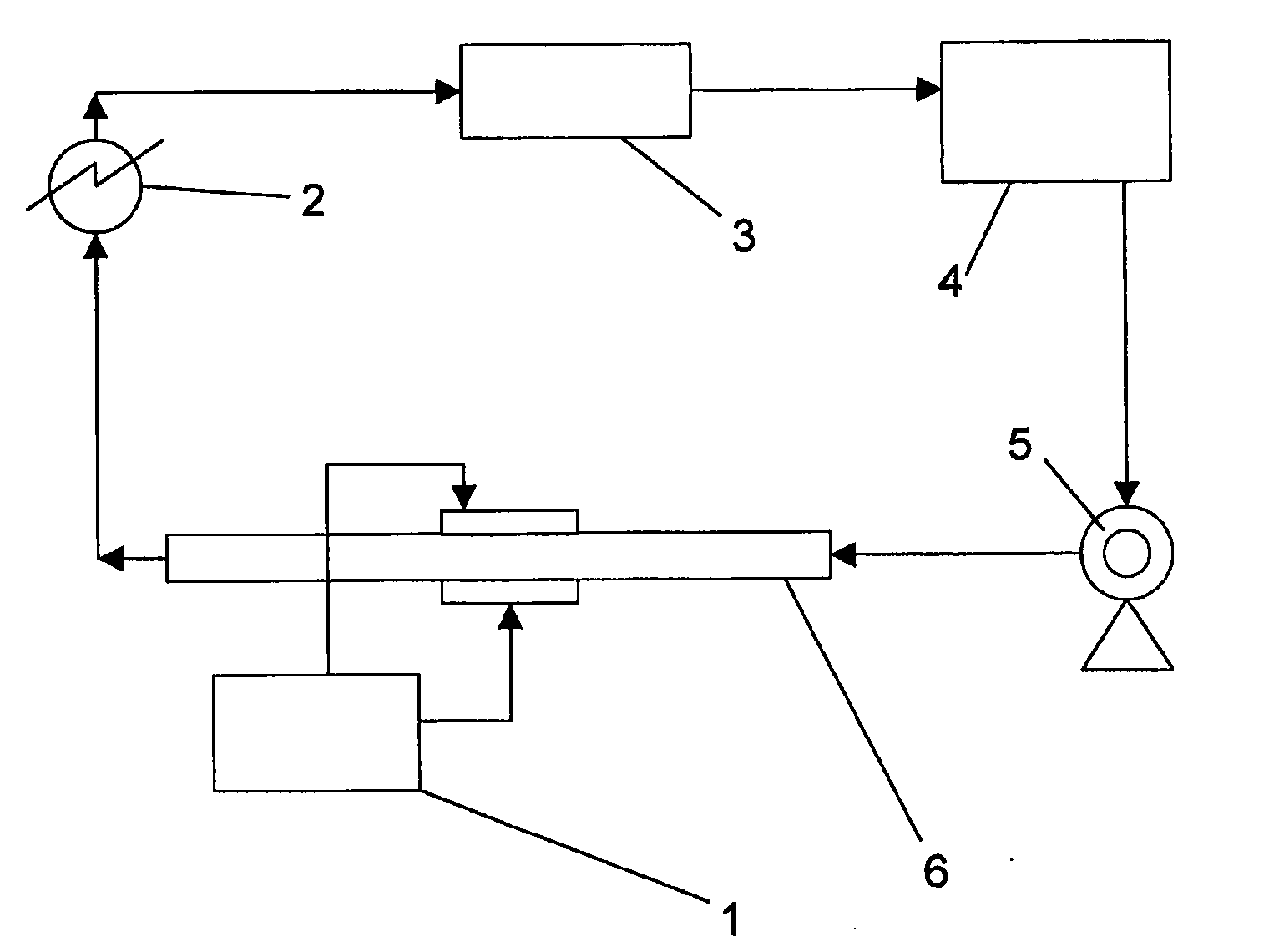
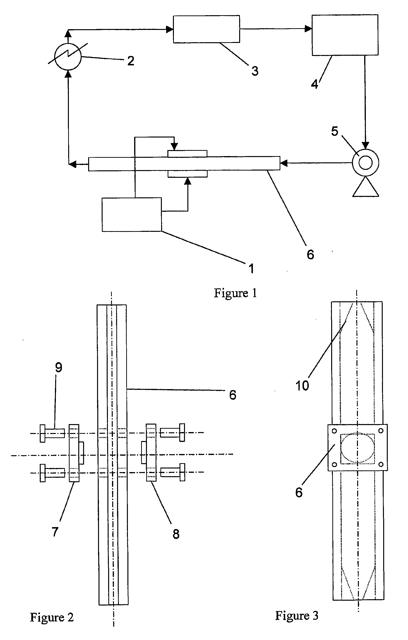
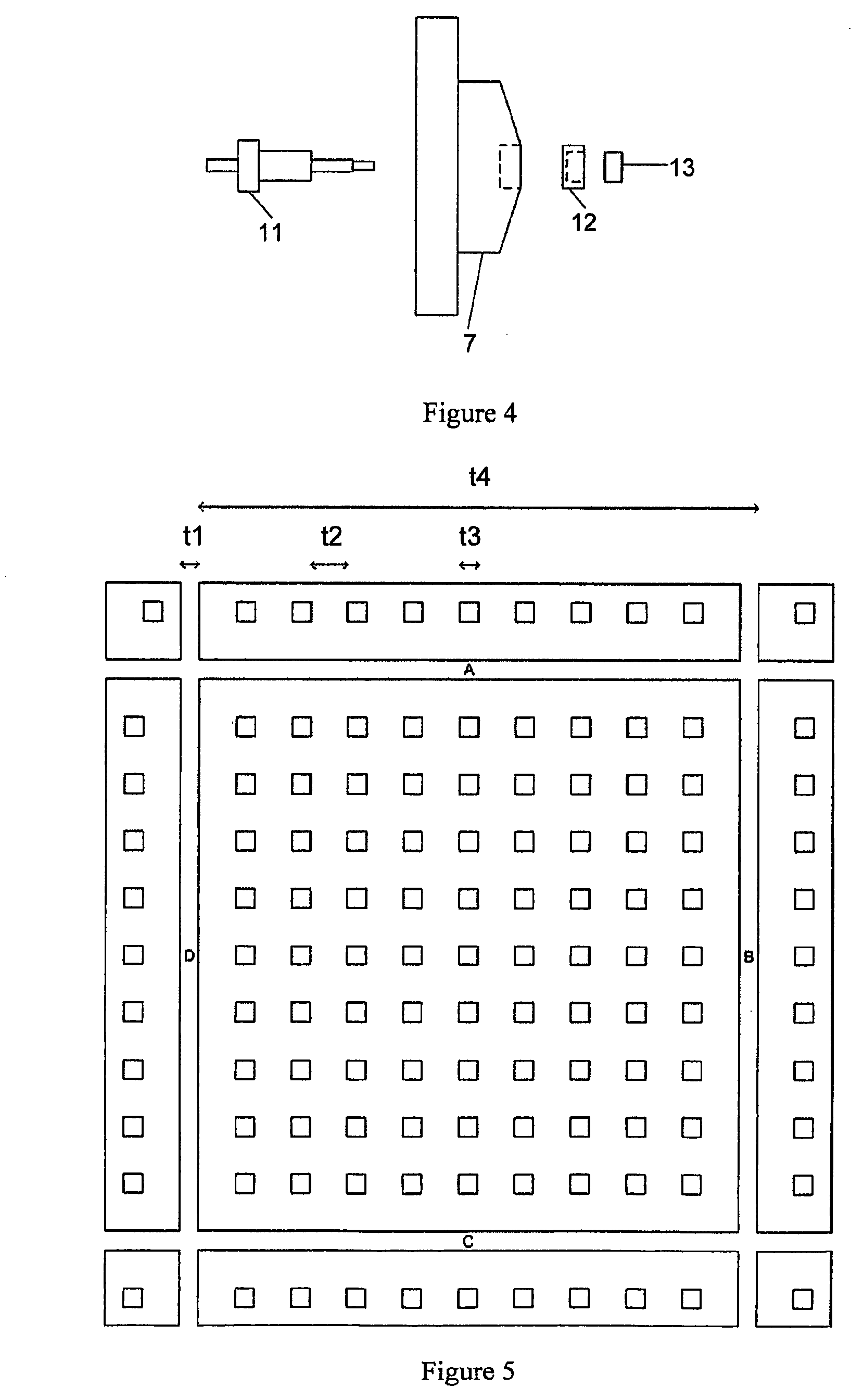
[0039]The vertical flow system for the main etching experiments has been described in literature for electrodeposition experiments (Meuleman, W. R. A., et al., J. Electrochem. Soc. 149, C479-C486 (2002); Dulal, S. M. S. I., et al., Electrochim. Acta, 49, 2041-2049 (2004)). The design of the flow cell, which is shown in FIGS. 2 and 3, was based on a model previously constructed by Roy et al. (Roy, S., et al., Chem. Eng. Science, 56, 5025 (2001)). The flow system, which is illustrated in FIG. 1, consisted of the flow cell 6 with two electrode holders, one for the cathode 7 and one for the anode 8, a heat exchanger 2, a filter unit / settling tank 3, an electrolyte reservoir 4, magnetically coupled pump 5, and a flow meter (not shown). The power supply 1 is coupled to the anode and cathode.

[0040]The cross-section of the flow cell as seen in FIG. 2 was rectangular and the electrolyte circulated upwards through the channel. The electrolyte was stored in a reservoir 4 and the velocity of th...


PUM

PropertyMeasurementUnit
Lengthaaaaaaaaaa
Molar densityaaaaaaaaaa
Timeaaaaaaaaaa

Abstract

A method of depositing or etching a micro- or nano-scale pattern on a work piece is disclosed, including the steps of: (a) placing the work piece in an electrochemical reactor in close proximity to a patterned tool; (b) connecting the work piece such that it is the anode if is to be etched or the cathode if it is to be deposited, and the patterned tool such that it is the counter electrode; (c) pumping electrolytic fluid necessary for the electrolytic operation of the cell formed between the two electrodes; and (d) applying a current across the electrodes to etch or deposit the work piece.

Description

[0001]This application is a National stage filing under 35 U.S.C. §371 of International Application No. PCT / GB2005 / 002795, filed on Jul. 19, 2005, which in turn claims priority to British Application No. 0416600.5, filed Jul. 24, 2004, the entire contents of which are incorporated herein by reference.FIELD[0002]This invention relates to a process, which can be used to selectively electrochemically deposit, or etch, micro patterns in various substrate materials, preferentially for the fabrication of micro-devices, nano-devices, and the like.BACKGROUND[0003]In the discussion that follows, reference is made to certain structures and / or methods. However, the following references should not be construed as an admission that these structures and / or methods constitute prior art. Applicants expressly reserve the right to demonstrate that such structures and / or methods do not qualify as prior art.[0004]Micro- and nano-machined devices are used in a variety of industries including electronics...

Claims


Application Information

Patent Timeline
IPC IPC(8): C23F1/00C25D5/02C25D5/08C25D17/12C25F3/14
CPCC25D5/022C25D5/08C25D17/12C25F3/14
Inventor ROY, SUDIPTA
Owner NEWCASTLE UPON TYNE UNIV OF
Why Eureka
Try Eureka