ZnO-BASED THIN FILM TRANSISTOR AND METHOD OF MANUFACTURING THE SAME

a thin film transistor and zno-based technology, applied in the field of zno-based thin film transistors, can solve the problems of reducing reliability, reducing the application range of existing a-si tfts, and degrading of -si tfts, and achieve the effect of effectively preventing the damage that occurs in the channel layer

a thin film transistor and zno-based technology, applied in the field of zno-based thin film transistors, can solve the problems of reducing reliability, reducing the application range of existing a-si tfts, and degrading of -si tfts, and achieve the effect of effectively preventing the damage that occurs in the channel layer

US20080283831A1Inactive Publication Date: 2008-11-20SAMSUNG ELECTRONICS CO LTD

Image

  • ZnO-BASED THIN FILM TRANSISTOR AND METHOD OF MANUFACTURING THE SAME
  • ZnO-BASED THIN FILM TRANSISTOR AND METHOD OF MANUFACTURING THE SAME
  • ZnO-BASED THIN FILM TRANSISTOR AND METHOD OF MANUFACTURING THE SAME

Examples


Embodiment Construction

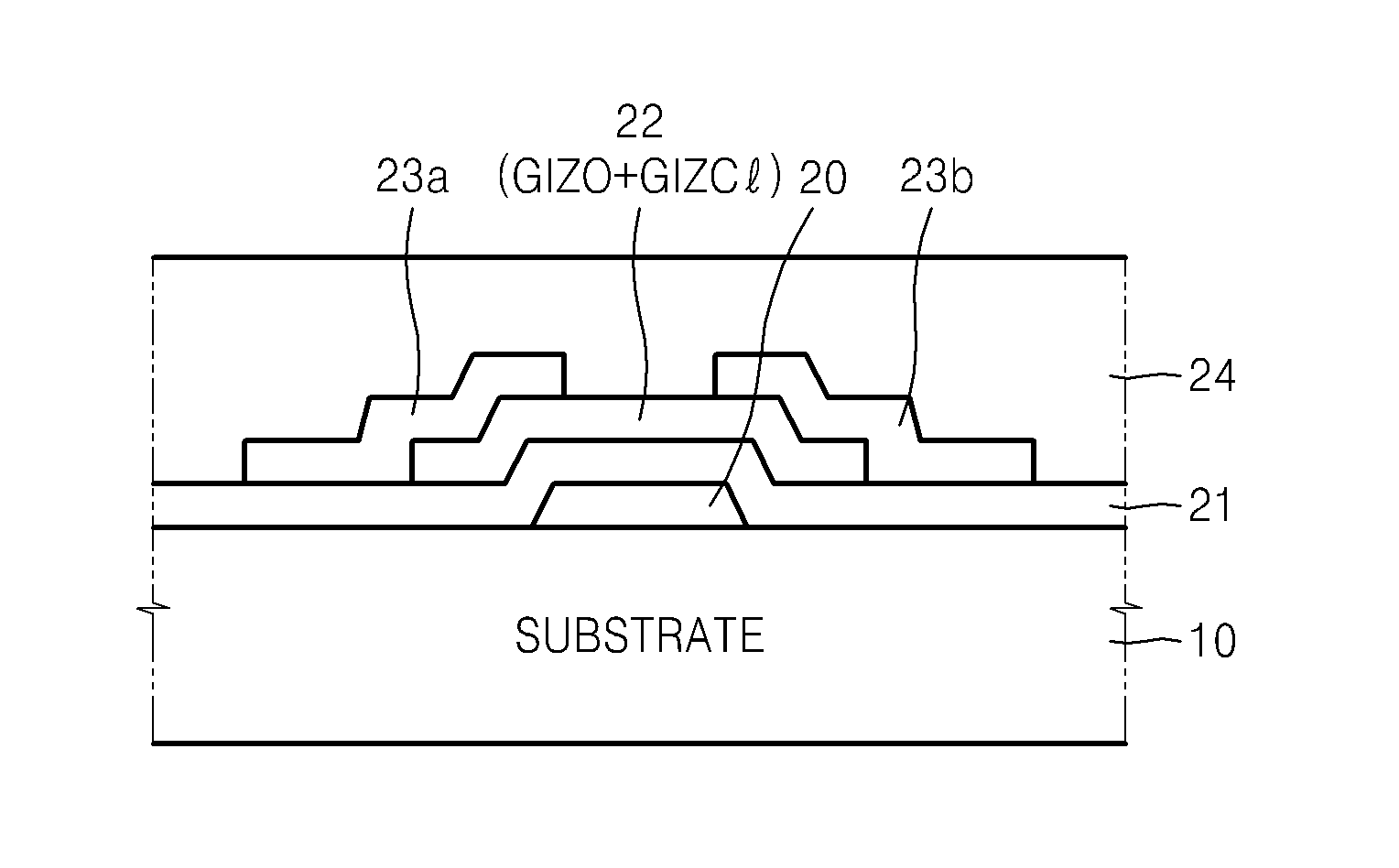
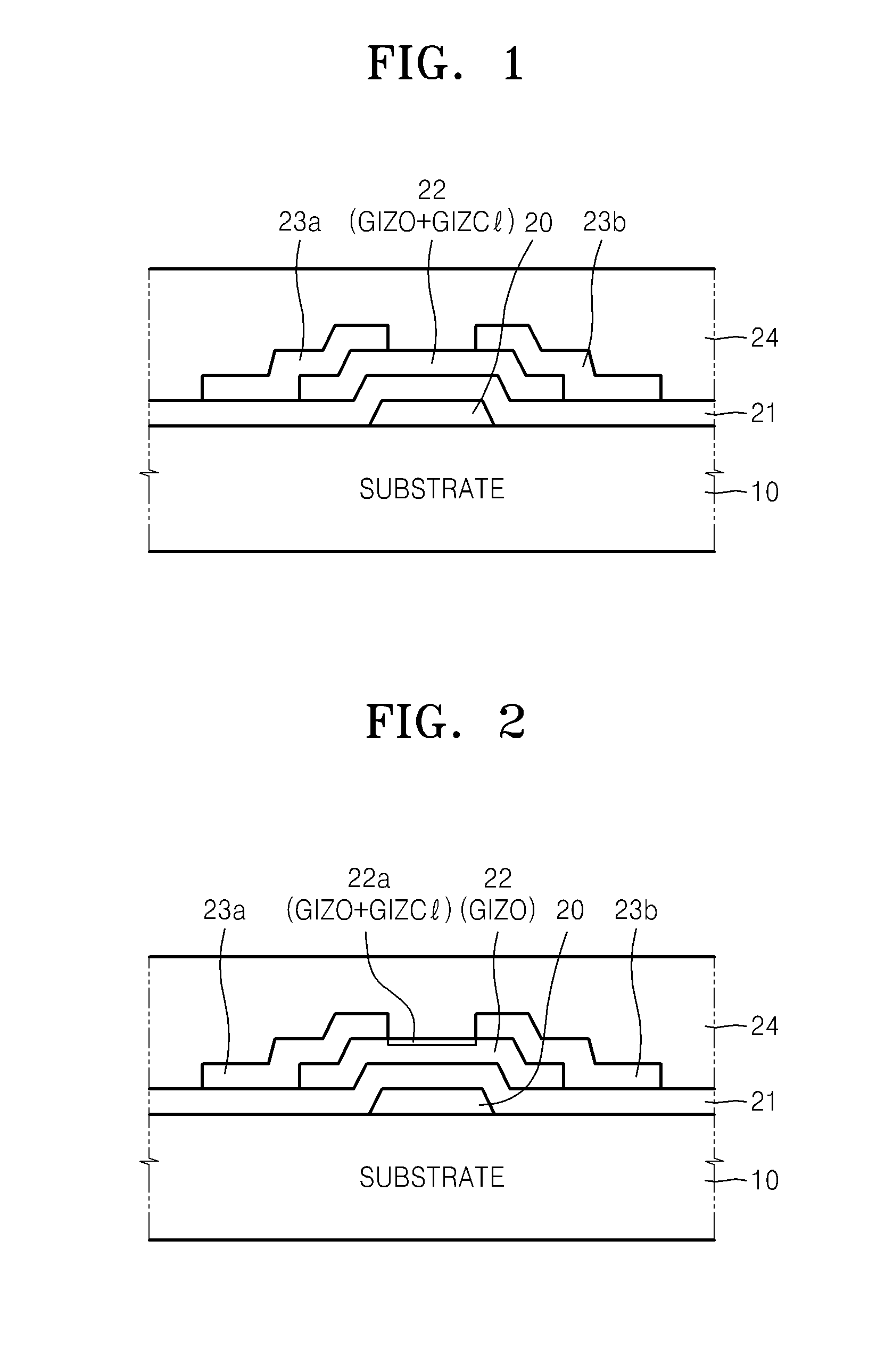
[0029]The present invention will now be described more fully with reference to the accompanying drawings, in which exemplary embodiments of the invention are shown.

[0030]It will be understood that when an element or layer is referred to as being “on,”“interposed,”“disposed,” or “between” another element or layer, it can be directly on, interposed, disposed, or between the other element or layer or intervening elements or layers may be present.

[0031]It will be understood that, although the terms first, second, third, and the like may be used herein to describe various elements, components, regions, layers and / or sections, these elements, components, regions, layers and / or sections should not be limited by these terms. These terms are only used to distinguish one element, component, region, layer or section from another element, component, region, layer or section. Thus, first element, component, region, layer or section discussed below could be termed second element, component, regio...


PUM


Abstract

A ZnO-based thin film transistor (TFT) is provided herein, as is a method of manufacturing the TFT. The ZnO-based TFT has a channel layer that comprises ZnO and ZnCl, wherein the ZnCl has a higher bonding energy than ZnO with respect to plasma. The ZnCl is formed through the entire channel layer, and specifically is formed in a region near THE surface of the channel layer. Since the ZnCl is strong enough not to be decomposed when exposed to plasma etching gas, an increase in the carrier concentration can be prevented. The distribution of ZnCl in the channel layer, may result from the inclusion of chlorine (Cl) in the plasma gas during the patterning of the channel layer.

Description

CROSS-REFERENCE TO RELATED PATENT APPLICATION[0001]This application claims the benefit of Korean Patent Application No. 10-2007-0048310, filed on May 17, 2007, in the Korean Intellectual Property Office, the disclosure of which is incorporated herein in its entirety by reference.BACKGROUND OF THE INVENTION[0002]1. Field of the Invention[0003]The disclosure relates to a ZnO-based thin film transistor (TFT) and a method of manufacturing the same.[0004]2. Description of the Related Art[0005]Televisions (“TV”s) are the main applications for the rapidly progressing field of flat panel displays. While liquid crystal displays (“LCD”s) are the most widely used displays for TVs, many attempts have been made to use organic light-emitting diodes (“OELD”s) for TVs. The development of displays for TVs has moved toward a focus on the incorporation of large screens, digital information displays (“DID”), low cost, as well as a high level of quality in the moving image, resolution, brightness, contr...

Claims


Application Information

Patent Timeline
20 Nov 2008
Publication
US20080283831A1
IPC
H01L29/227; H01L21/34
CPC
H01L29/7869; H01L29/78696
Inventors
RYU, MYUNG-KWAN; KIM, JUN-SEONG