On-die system and method for controlling termination impedance of memory device data bus terminals

a data bus terminal and memory device technology, applied in the field of memory devices, can solve the problems of adversely affecting timing margins, negative impact on memory device performance, and performance in this regard less than optimal

Active Publication Date: 2008-11-20
MICRON TECH INC
View PDF8 Cites 29 Cited by
  • Summary
  • Abstract
  • Description
  • Claims
  • Application Information

AI Technical Summary

Problems solved by technology

Subtle variations in signal timing and operating conditions can negatively impact memory device performance.
One factor that can adversely affect timing margins is reflection of signals in conductors through which data signals are coupled.
These reflected read and write data signals can remain present on the data bus as subsequent data signals are coupled through the data bus, and they can alter in spurious manner the timing of transitions of these subsequent data signals or the amplitude of these subsequent data signals.
However, its performance in this regard is less than optimum because the resist...

Method used


Image

  • On-die system and method for controlling termination impedance of memory device data bus terminals
  • On-die system and method for controlling termination impedance of memory device data bus terminals
  • On-die system and method for controlling termination impedance of memory device data bus terminals

Examples


Embodiment Construction

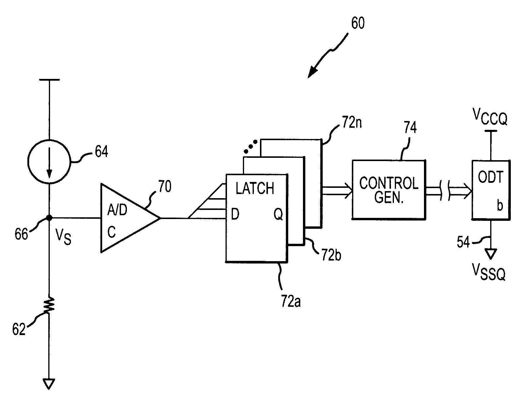
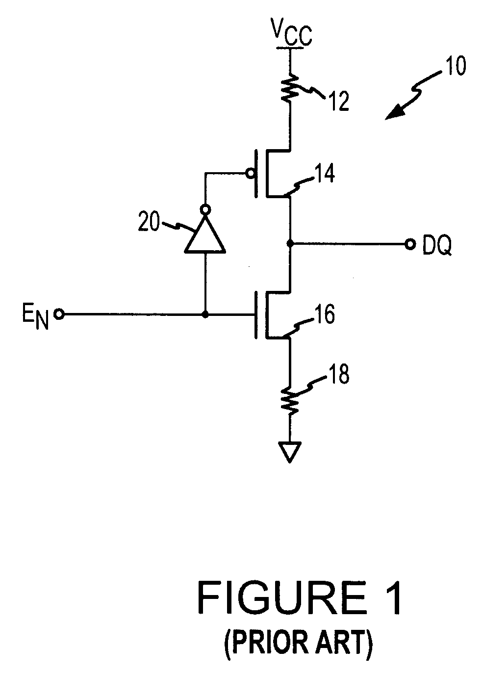
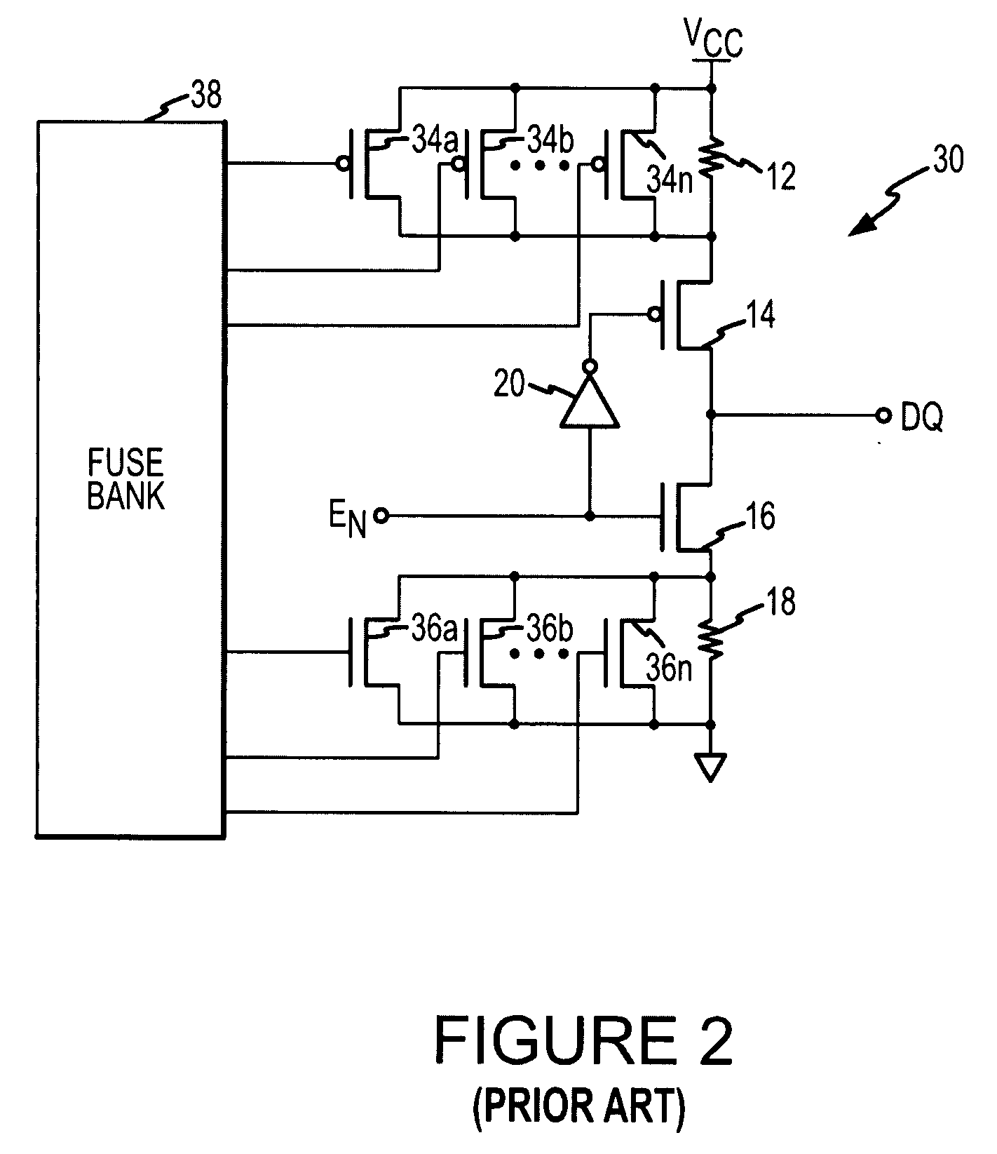
[0023]An ODT system 50 according to one example of the invention is shown in FIG. 3. The ODT system 50 will generally be fabricated on the same chip as a memory device with which the ODT system 50 is used. The ODT system 50 includes an ODT circuit 54, which may be identical to the ODT circuit 30 shown in FIG. 2 except that the fuse bank 38 is omitted. Instead of programming the ODT circuit 50 with signals from a fuse bank, the ODT circuit 54 is programmed by signals from a termination resistance determining circuit 56. The termination resistance determining circuit 56 determines the termination impedance provided by the termination resistors 12, 18 (FIG. 2) without any of the transistors 34a,b . . . n, 36a,b . . . n turned ON. As explained in greater detail below, the termination resistance determining circuit 56 determines the termination impedance either directly, such as by measuring the resistance of a polysilicon resistor like those used in the ODT circuit 54, or indirectly by ...


PUM


Abstract

A system for controlling the termination impedance of memory device data bus terminals is fabricated on the same die as the memory device. The system includes a termination resistor connected to each data bus terminal, which is connected in parallel with several transistors that are selectively turned on to adjust the termination impedance. The transistors are controlled by a circuit that determines the resistance of the termination resistor and turns on the correct number of transistor to properly set the termination impedance. In one example, the resistance of the termination resistor is determined by directly measuring a resistor of the same type as the termination resistor. In another example, the resistance of the termination resistor is determined indirectly by measuring parameters that affect the resistance of the termination resistor. In either case, the system can maintain the termination impedance of the data bus terminals constant despite changes in the termination resistor.

Description

TECHNICAL FIELD[0001]This invention relates to memory devices, and more specifically, to controllably adjusting the termination impedance of data bus terminals that are used to couple write data to and read data from the memory data.BACKGROUND OF THE INVENTION[0002]Memory devices are typically assembled into memory modules that are used in a computer system. These memory modules typically include single in-line memory modules (SIMMs) having memory devices on one side of the memory module, and dual in-line memory modules (DIMMs) having memory devices on both sides of the memory module. The memory devices of a memory module are accessed in groups. Each of the groups are commonly referred to as “ranks,” with single-sided DIMMs typically having one rank of memory devices and double-sided DIMMs having two ranks of memory devices, one rank on either side of the memory module.[0003]Each of the memory devices of a memory module receives a set of signals, which is generated by a memory contr...

Claims


Application Information

Patent Timeline
IPC IPC(8): H03K19/003
CPCH04L25/0278H03K19/017545H04L25/028
Inventor KAO, DAVID
Owner MICRON TECH INC
Why Eureka
Try Eureka