Wafer level lens arrays for image sensor packages and the like, image sensor packages, and related methods

a technology for image sensor packages and wafers, applied in the field of wafer level lens arrays for image sensor packages, can solve problems such as substantial waste of materials

Inactive Publication Date: 2008-11-27
APTINA IMAGING CORP
View PDF21 Cites 237 Cited by
  • Summary
  • Abstract
  • Description
  • Claims
  • Application Information

AI Technical Summary

Problems solved by technology

For example, the extent to which the packages can be at least partially, if not completely, fabricated at the wafer level is a substantial cost consideration.
Furthermore, if the package design or fabrication approach, even if conducted at the wafer level, necessitates that all of the image sensor semiconductor dice located thereon be packaged regardless of whether a significant number of the dice are defective, a substantial waste of materials results.

Method used


Image

  • Wafer level lens arrays for image sensor packages and the like, image sensor packages, and related methods
  • Wafer level lens arrays for image sensor packages and the like, image sensor packages, and related methods
  • Wafer level lens arrays for image sensor packages and the like, image sensor packages, and related methods

Examples


Embodiment Construction

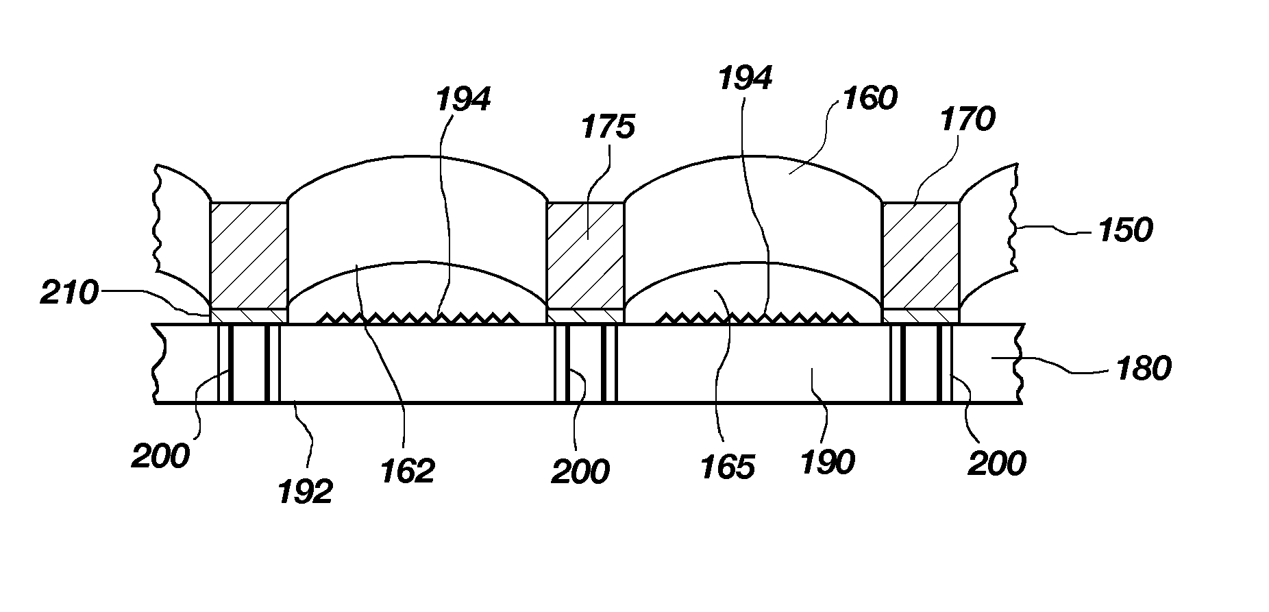
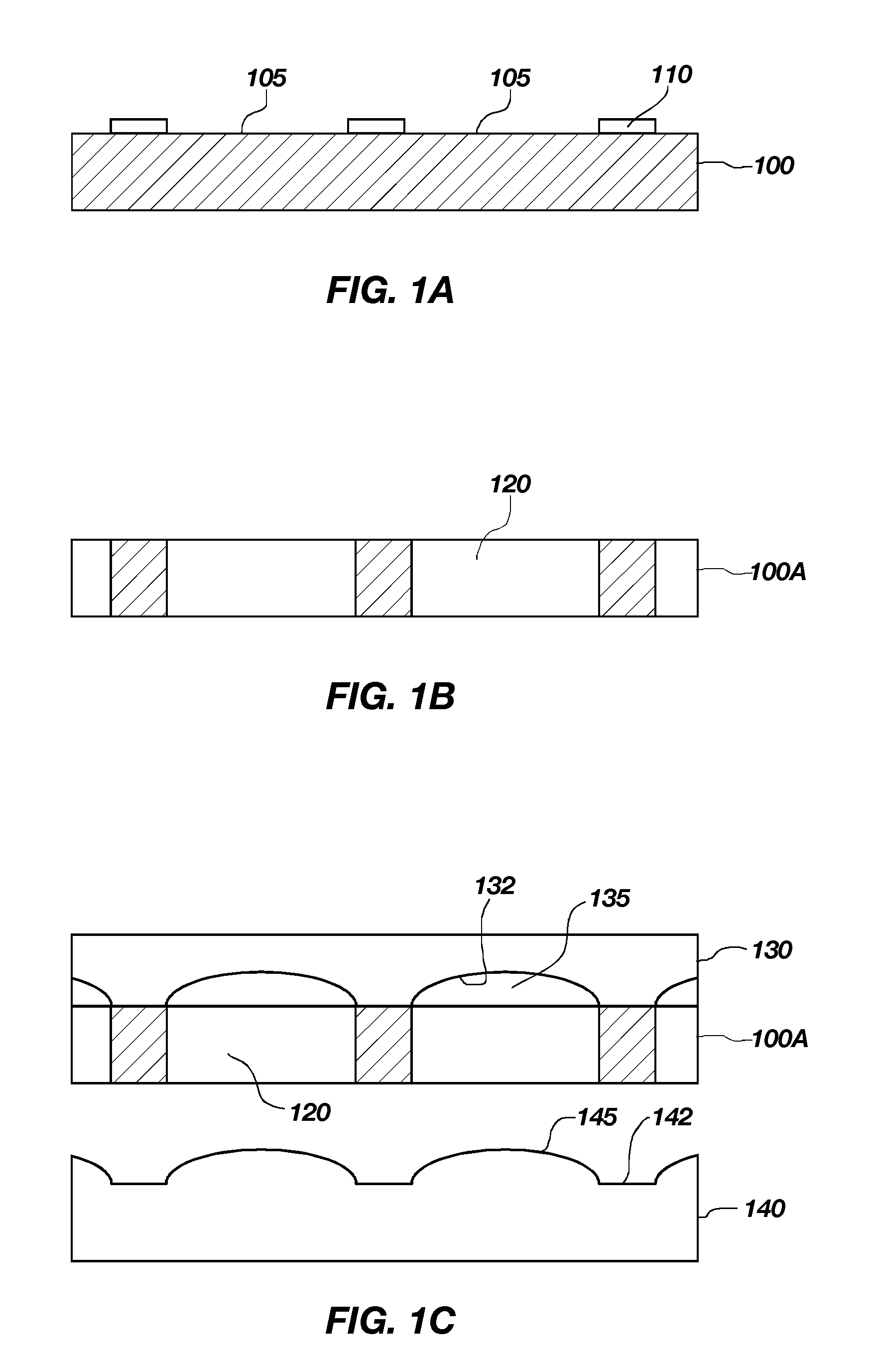
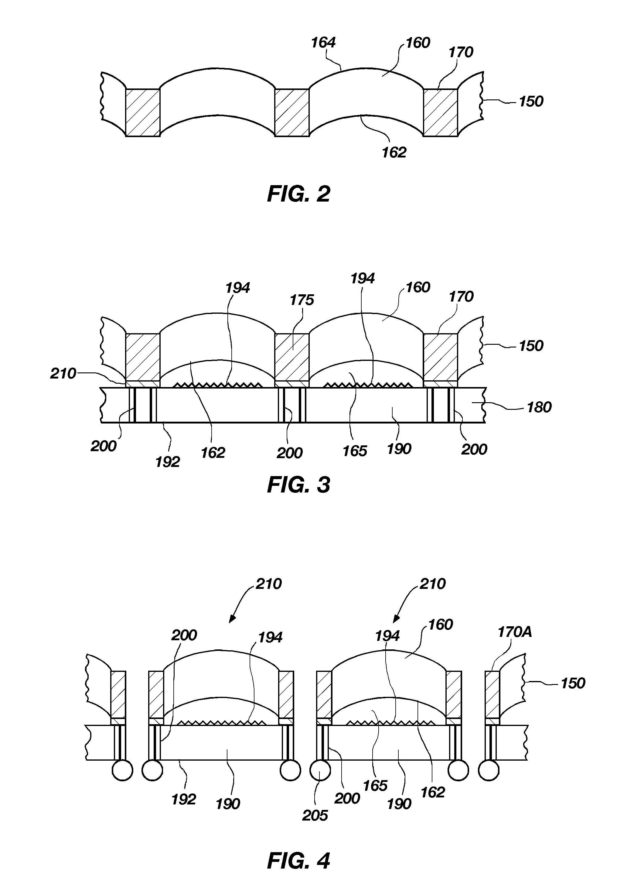
[0022]Referring in general to the accompanying drawings, various aspects of the present invention are illustrated to show embodiments of semiconductor package structures and methods for assembly of such package structures. Common elements of the illustrated embodiments are designated with like reference numerals. It should be understood that the figures presented are not meant to be illustrative of actual views of any particular port ion of a particular semiconductor package structure, but are merely idealized schematic representations which are employed to more clearly and fully depict the invention.

[0023]FIGS. 1A through 1C illustrate a method of forming a lens array at the wafer or other bulk substrate level. A substrate 100 is provided with patterned photoresist 110 thereon. The substrate 100 may be sized and shaped like a wafer for use in processing by existing semiconductor fabrication equipment. The substrate 100 may comprise, by way of example, a silicon or borosilicate mate...


PUM

PropertyMeasurementUnit
optical color filtering propertiesaaaaaaaaaa
optically activeaaaaaaaaaa
optical filtering propertiesaaaaaaaaaa

Abstract

Image sensor packages, lenses therefore, and methods for fabrication are disclosed. A substrate having through-hole vias may be provided, and an array of lenses may be formed in the vias. The lenses may be formed by molding or by tenting material over the vias. An array of lenses may provide a color filter array (CFA). Filters of the CFA may be formed in the vias, and lenses may be formed in or over the vias on either side of the filters. A substrate may include an array of microlenses, and each microlens of the array may correspond to a pixel of an associated image sensor. In other embodiments, each lens of the array may correspond to an imager array of an image sensor. A wafer having an array of lenses may be aligned with and attached to an imager wafer comprising a plurality of image sensor dice, then singulated to form a plurality of image sensor packages.

Description

FIELD OF THE INVENTION[0001]The present invention relates to lenses for image sensor packages, wafer level structures in the fabrication thereof and components and fabrication methods therefore. More particularly, the invention pertains to methods for fabricating lenses at a wafer or other bulk substrate level for packaging radiation sensing or emitting devices, as well as cameras and the like including the same, and lenses at the wafer or other bulk substrate level in the fabrication.BACKGROUND OF THE INVENTION[0002]State of the Art: Semiconductor die-based image sensors are well known to those having skill in the electronics / photonics art and, in a miniaturized configuration, are useful for capturing electromagnetic radiation (e.g., visual, IR or UV) information in digital cameras, personal digital assistants (PDA), internet appliances, cell phones, test equipment, and the like, for viewing, further processing or both. For commercial use in the aforementioned extremely competitive...

Claims


Application Information

Patent Timeline
Patent Type & Authority Applications(United States)
IPC IPC(8): H01L31/0232B29D11/00H01L21/00
CPCB29D11/00375H01L27/14618H01L27/14625H01L27/14632H01L27/14685H01L2924/0002B29D11/00307H01L2924/00
Inventor OLIVER, STEVEKIRBY, KYLE K.FARNWORTH, WARREN M.HIATT, WILLIAM M.AKRAM, SALMAN
Owner APTINA IMAGING CORP
Why Eureka
Try Eureka