
Liquid crystal device and manufacturing method therefor, and electronic apparatus

a technology of liquid crystal devices and manufacturing methods, applied in the direction of optics, instruments, non-linear optics, etc., can solve the problems of weak azimuth along which liquid crystals fall when voltage is applied, display defects, and interaction in the azimuth, and achieve excellent display characteristics

Inactive Publication Date: 2008-11-27
SEIKO EPSON CORP
View PDF3 Cites 6 Cited by
  • Summary
  • Abstract
  • Description
  • Claims
  • Application Information

AI Technical Summary

Benefits of technology

[0025]An aspect of the invention is to provide a liquid crystal device that has good contrast characteristics and in which display defects such as a disclination are prevented, a manufacturing method thereof, and an electronic apparatus.

Problems solved by technology

However, in the vertical alignment mode, liquid crystals align themselves perpendicularly to the surface of a substrate, and the interaction in the azimuth along which the liquid crystals fall when voltage is applied is weak.
If a disclination occurs, display defects such as irregularity in brightness, decrease in contrast, and image stickingbecome visible.
In this method, however, when the liquid crystal molecules are tilted by a few degrees, birefringence of liquid crystal molecules occurs.
The birefringence causes light leakage.
Therefore, a high-contrast display caused by vertical alignment at 90 degrees with respect to the substrate surface is not achieved.
Actually, the orientation of liquid crystals often cannot be controlled according to the conditions, and therefore the liquid crystal device in this example cannot be used, i.e., a disclination occurs in some cases.

Method used


Image

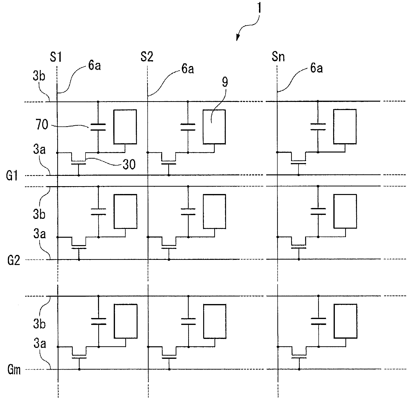
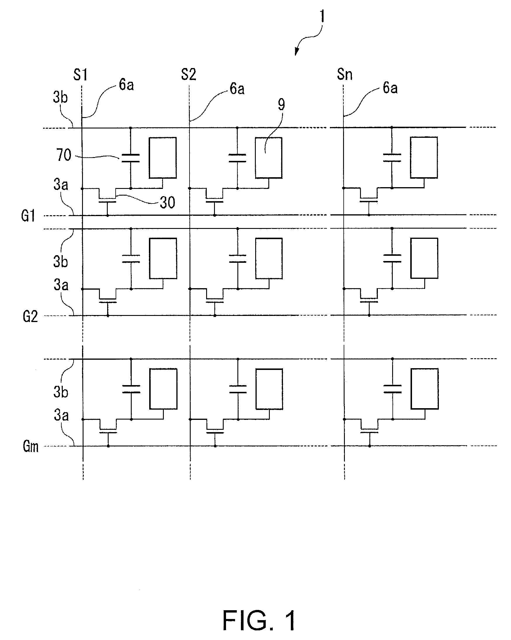
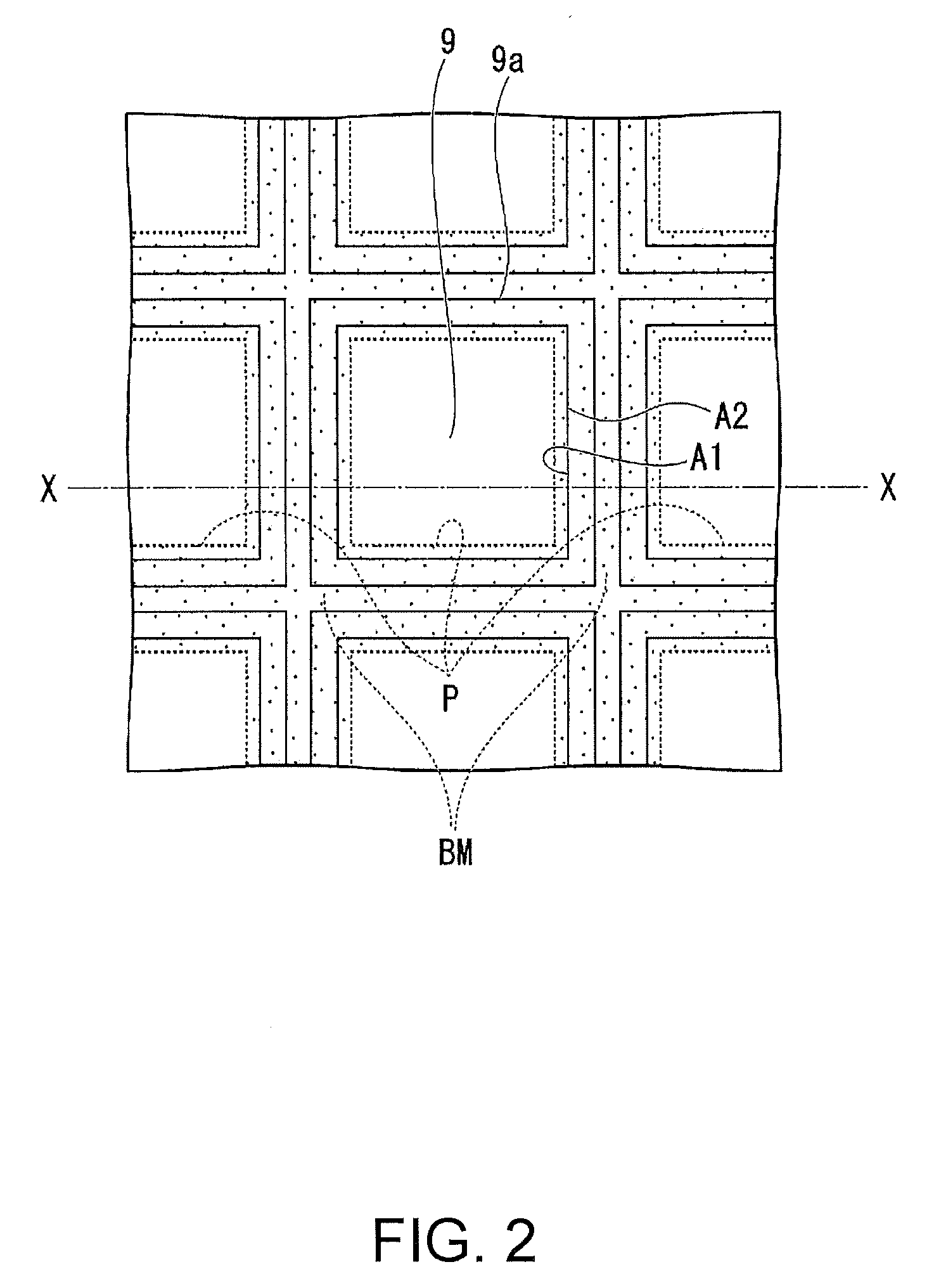
  • Liquid crystal device and manufacturing method therefor, and electronic apparatus
  • Liquid crystal device and manufacturing method therefor, and electronic apparatus
  • Liquid crystal device and manufacturing method therefor, and electronic apparatus

Examples


first example

[0197]In this example, transmission simulations were performed for a plurality of liquid crystal devices that differed from one another in the pretilt angle LP ranging from 12 to 15 degrees under the conditions that the distance EG between pixel electrodes was 0.2 μm, the overlapping width of a portion of the second area A2 that projected on the perimeter 9b was 0.1 μm, and the cell gap d of the liquid crystal panel was 2.5 μm.

[0198]FIGS. 9 to 12 illustrate the results of the transmission simulations for liquid crystal devices.

[0199]As illustrated in FIG. 9, in the case of a pretilt angle LP of 12 degrees, a disclination did not occur in a pixel (display region P) and a sufficient transmittance was obtained in the pixel.

[0200]However, as illustrated in FIGS. 10 to 12, it was found that a disclination occurred from an end of the pixel if the pretilt angle LP of the liquid crystals 52 exceeded 12 degrees.

[0201]It was found that the place where a disclination occurred varied depending ...

second example

[0205]In this example, transmission simulations were performed under the condition that the distance EG between pixel electrodes was 1.2 μm.

[0206]FIG. 13 illustrates the result of the transmission simulation for a liquid crystal device having a pretilt angle LP of 14 degrees.

[0207]In the configuration of the above first example, if the pretilt angle LP exceeded 12 degrees, a disclination occurred.

[0208]However, as illustrated in FIG. 13, if the distance EG between pixel electrodes was 1.2 μm, a disclination did not occur in the case of a pretilt angle LP of 14 degrees.

[0209]Further, when a transmission simulation was performed for a liquid crystal device having a pretilt angle LP larger than 14 degrees, a disclination occurred in the case of a pretilt angle LP of 35 degrees as illustrated in FIG. 14.

[0210]In other words, it was found that as the distance EG between pixel electrodes increased, the upper limit of a desired pretilt angle LP increased.

third example

[0211]Next, transmission simulations were performed for more precise liquid crystal devices.

[0212]In this example, transmission simulations were performed for a plurality of liquid crystal devices that differed from one another in the cell gap d (d=1.5 μm, 2.0 μm, and 2.5 μm) under the conditions that the distance EG between pixel electrodes was 0.05 μm, the overlapping width LPW was 0.2 μm, and the pretilt angle LP was 12 degrees.

[0213]FIGS. 15 to 17 illustrate the results of the transmission simulations for these liquid crystal devices.

[0214]As illustrated in FIG. 15, in the case of a cell gap d of 1.5 μm, a disclination did not occur.

[0215]However, as illustrated in FIGS. 16 and 17, it was found that if the cell gap d was 2.0 μm or more, a disclination occurred approximately at the center of the pixel.

[0216]In FIG. 15, since the vertical electric field intensity increases as compared to a liquid crystal device having a large cell gap d as illustrated in FIGS. 16 and 17, the direc...


PUM

PropertyMeasurementUnit
pretilt anglesaaaaaaaaaa
pretilt angleaaaaaaaaaa

Abstract

A liquid crystal device includes: a first substrate; a second substrate that is disposed facing the first substrate; a liquid crystal layer that is sandwiched between the first substrate and the second substrate and is composed of a liquid crystal exhibiting, in an initial alignment state thereof, a vertical alignment and having negative dielectric anisotropy; a light shielding film that is formed on a side of the liquid crystal layer on the first substrate and that corresponds to a non-display region and defining a display region; a pixel electrode that is disposed, on the first substrate, from the display region with a periphery projecting on the light shielding film; a vertical alignment film that is disposed, on the pixel electrode, only in the display region or from the display region with a periphery projecting in the non-display region; and a horizontal alignment film that is disposed, in an area without the vertical alignment film above the light shielding film, with a periphery projecting on the pixel electrode.

Description

BACKGROUND OF THE INVENTION[0001]1. Technical Field[0002]The present invention relates to a liquid crystal device and a manufacturing method therefor, and an electronic apparatus.[0003]2. Related Art[0004]As an apparatus for displaying an image on a large screen using a liquid crystal device, there is a liquid crystal projector.[0005]High luminance and high contrast are required for a projector. In this respect, a liquid crystal device of a vertical alignment mode can provide displays with high contrast.[0006]Recently, this mode have been increasingly employed as the liquid crystal alignment mode of a liquid crystal device for a projector.[0007]However, in the vertical alignment mode, liquid crystals align themselves perpendicularly to the surface of a substrate, and the interaction in the azimuth along which the liquid crystals fall when voltage is applied is weak.[0008]If a pixel potential is applied to a pixel electrode and a counter electrode, an electric field generated from an...

Claims


Application Information

Patent Timeline
Patent Type & Authority Applications(United States)
IPC IPC(8): G02F1/1337G02F1/1335
CPCG02F1/133512G02F1/133711G02F1/133753G02F2001/13373G02F2001/133738G02F2001/133742G02F2001/133757G02F1/13373G02F1/133738G02F1/133742G02F1/133757
Inventor KUROSAWA, RYUICHINAGAE, NOBUKAZUMIYASHITA, TAKESHI
Owner SEIKO EPSON CORP
Learn More