

Resin molded semiconductor device
a semiconductor and resin-based technology, applied in semiconductor devices, semiconductor/solid-state device details, electrical devices, etc., can solve the problems of particularly prone to receiving of the difficult detachment between the circuit board and the resin part at so as to reduce the stress to be applied to the four corner portions of the circuit board
- Summary
- Abstract
- Description
- Claims
- Application Information
AI Technical Summary
Benefits of technology
Problems solved by technology
Method used
Image

Examples
first embodiment
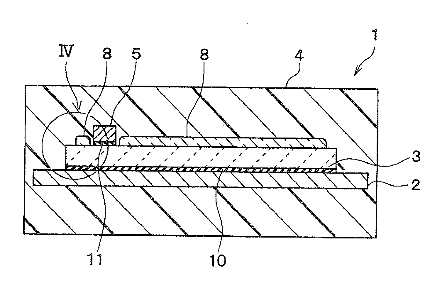
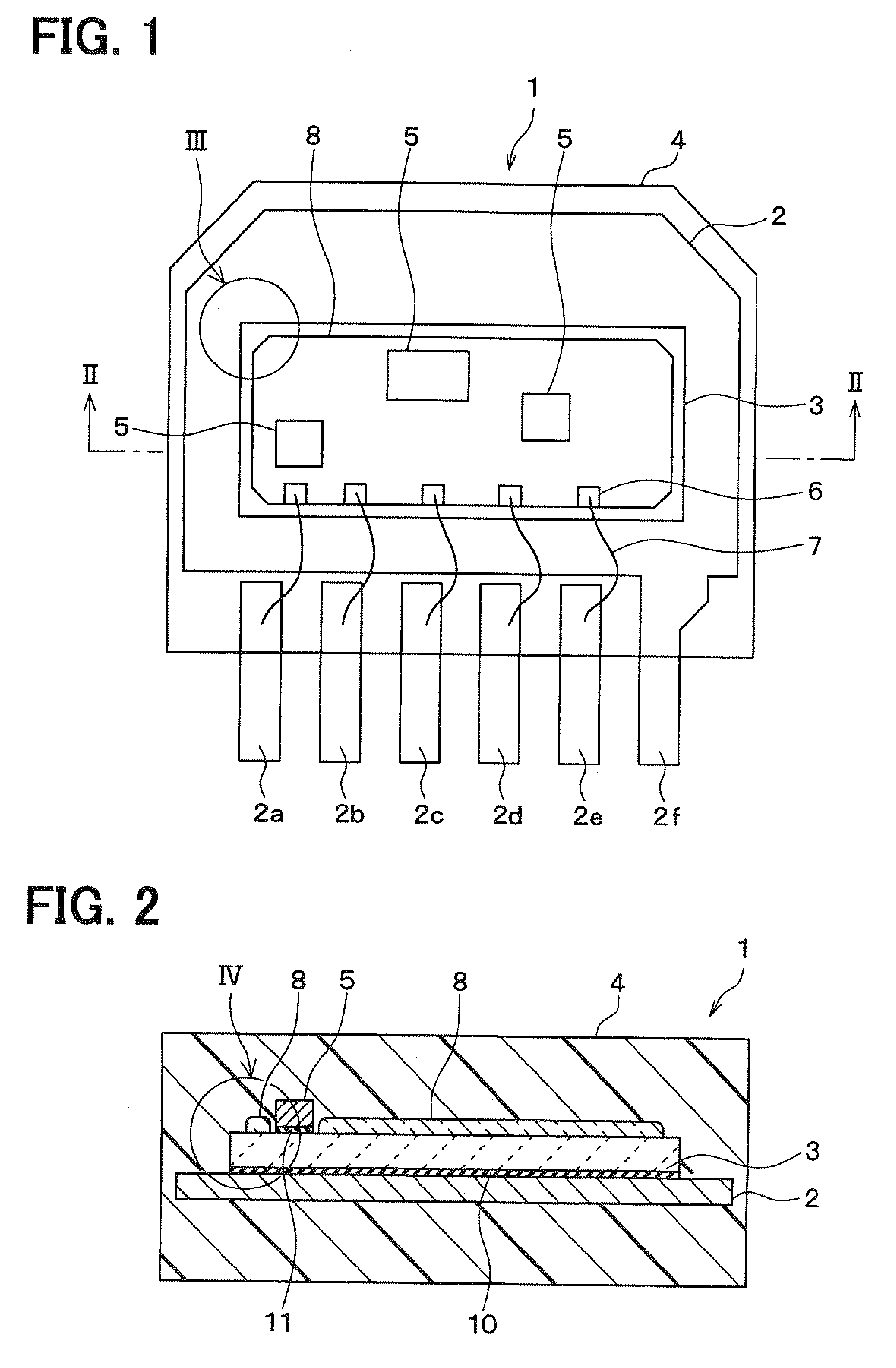
[0030]A semiconductor device 1 according to a first embodiment of the invention will be described with reference to FIGS. 1-4. The semiconductor device 1 can be suitably used for an ignition device for a vehicular engine (not shown) and can be attached to the vehicular engine directly. As shown in FIGS. 1 and 2, the semiconductor device 1 includes a lead frame 2 (wiring part) made of a conductive material, e.g., metal, a circuit board 3 attached to the lead frame 2 through adhesive agent 10, and a resin part 4 that seals the circuit board 3 and the lead frame 2. The lead frame 2 includes connector terminals 2a-2f. The connector terminals 2a-2f protrude to an outside of the resin part 4 and are configured to be electrically coupled with an external electronic device (not shown).
[0031]The circuit board 3 has a substrate made of ceramic, for example. On an upper surface of the substrate, a circuit wiring is pattern-formed. Mounted parts 5 are disposed on a predetermined portion of the ...
second embodiment
[0044]A semiconductor device 1 according to a second embodiment of the invention will be described with reference to FIGS. 5-7. In the semiconductor device 1 shown in FIGS. 5 and 6, a resin coating 9 is provided to cover the mounted parts 5 and protective coating glass 8 disposed on the circuit board 3. The resin coating 9 is made of polyamide, polyamide-imide, or polyimide, for example.
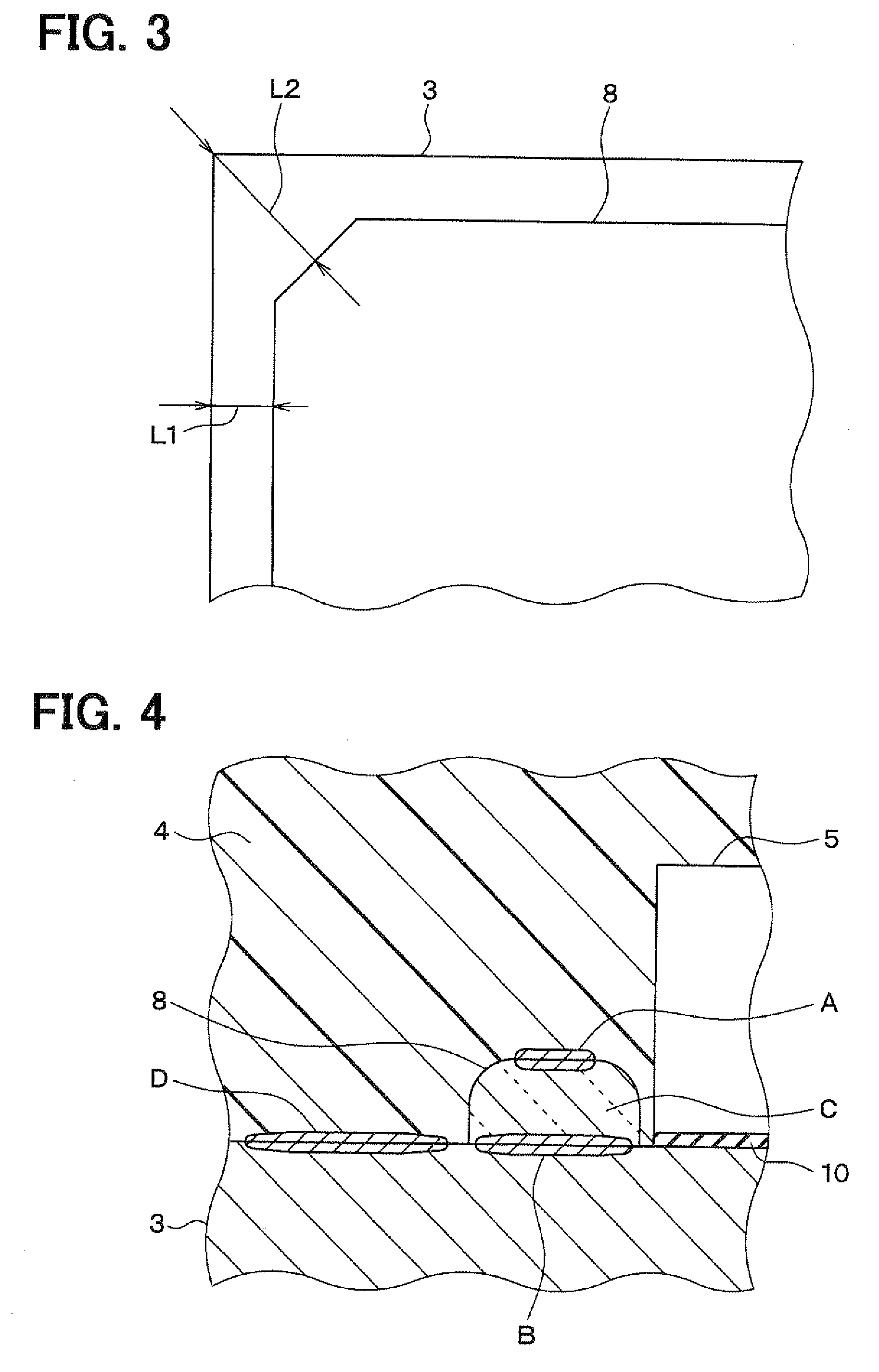
[0045]The resin coating 9 has an approximately rectangular shape that is smaller than the circuit board 3 and that has four sides and four chamfered corner portions. As shown in FIG. 7, the resin coating 9 is arranged in such a manner that an outer-peripheral end of the resin coating 9 is located between the outer-peripheral end of the protective coating glass 8 and each of the four sides of the circuit board 3. A third distance L3 between the outer-peripheral end of the resin coating 9 and each of the four sides of the circuit board 3 is larger than a predetermined distance. Thus, the resin coating ...
third embodiment
[0057]In a semiconductor device 1 according to a third embodiment of the invention, an alignment of the resin coating 9 with respect to the protective coating glass 8 is determined, as shown in FIG. 9. The other part of the semiconductor device 1 according to the third embodiment is almost similar with the semiconductor device 1 according to the second embodiment.
[0058]The resin coating 9 is arranged in such a manner that the outer-peripheral end of the resin coating 9 is located between the outer-peripheral end of the protective coating glass 8 and each of the four sides of the circuit board 3. In the present case, a fifth distance L5 from each side of the resin coating 9 to each side of the protective coating glass 8 is larger than a predetermined distance. Thus, a portion of the resin coating 9 is directly attached to the substrate of the circuit board 3. The fifth distance L5 is determined in such a manner that the resin coating 9 and the circuit board 3 is sufficiently contact ...
PUM
 Abstract
Description
Claims
Application Information