Method for testing multi-chip stacked packages

a technology of multi-chip stacking and packaging, which is applied in the direction of electronic circuit testing, measurement devices, instruments, etc., can solve the problems of reducing the yield of conventional semiconductor package tester pins, increasing the thickness and footprint of the overall package, and unable to use the tester for conventional semiconductor package pins, etc., to achieve the effect of easy integration into the tsv packaging process

Inactive Publication Date: 2013-03-28
POWERTECH TECHNOLOGY
View PDF13 Cites 29 Cited by
  • Summary
  • Abstract
  • Description
  • Claims
  • Application Information

AI Technical Summary

Benefits of technology

[0004]The main purpose of the present invention is to provide a method for testing multi-chip stacked packages to achieve fine-pitch probing of substrate-less chip cubes which can easily be integrated into TSV packaging processes.
[0005]The second purpose of the present invention is to provide a method for testing multi-chip stacked packages to test one or more substrate-less chip cubes before SMT on boards and to reduce the number of adhering steps of adhesive tapes to achieve lower packaging cost and to prevent SMT bonding bad substrate-less chip cube on boards.

Problems solved by technology

However, using a substrate increases overall package thickness and footprint.
However, bad chips are always randomly present within a wafer, therefore, wafer-to-wafer bonding would cause overall packaging yield of substrate-less chip cubes to drop.
Moreover, when a substrate is eliminated, the pitch between the external electrical electrodes or / and the testing electrodes of a chip cube is shrunk from a few hundred micrometer down below a hundred micrometer so that the existing pogo pins of a tester for conventional semiconductor packages can not be used.
The other one is to directly mount the substrate-less chip cube onto an interposer (normally made of Si) with fan-out circuitry and fan-out electrodes then load the interposer into a tester having pogo pins to perform testing where the overall testing cost is quite complicated and expensive.

Method used


Image

  • Method for testing multi-chip stacked packages
  • Method for testing multi-chip stacked packages
  • Method for testing multi-chip stacked packages

Examples


Embodiment Construction

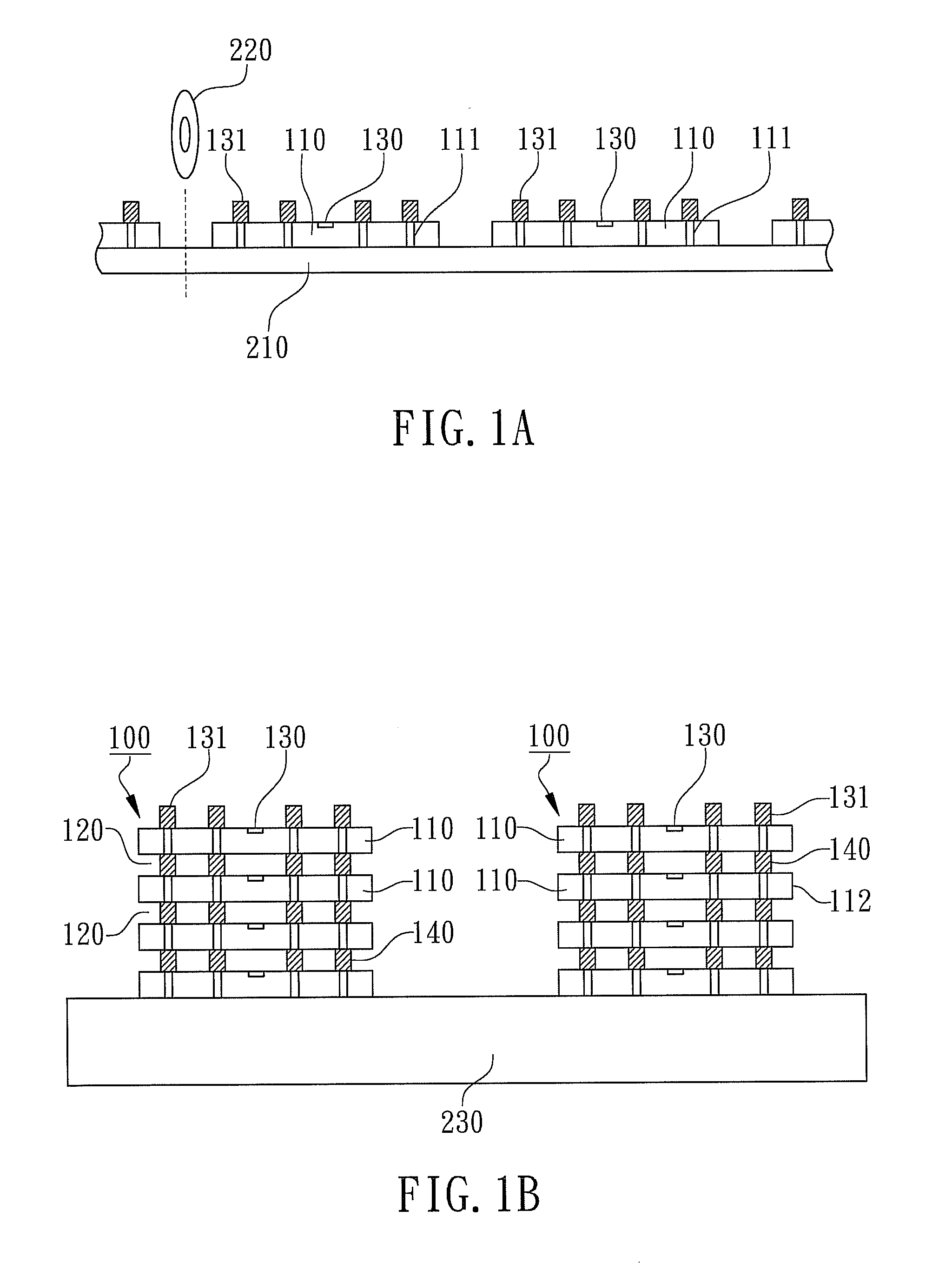
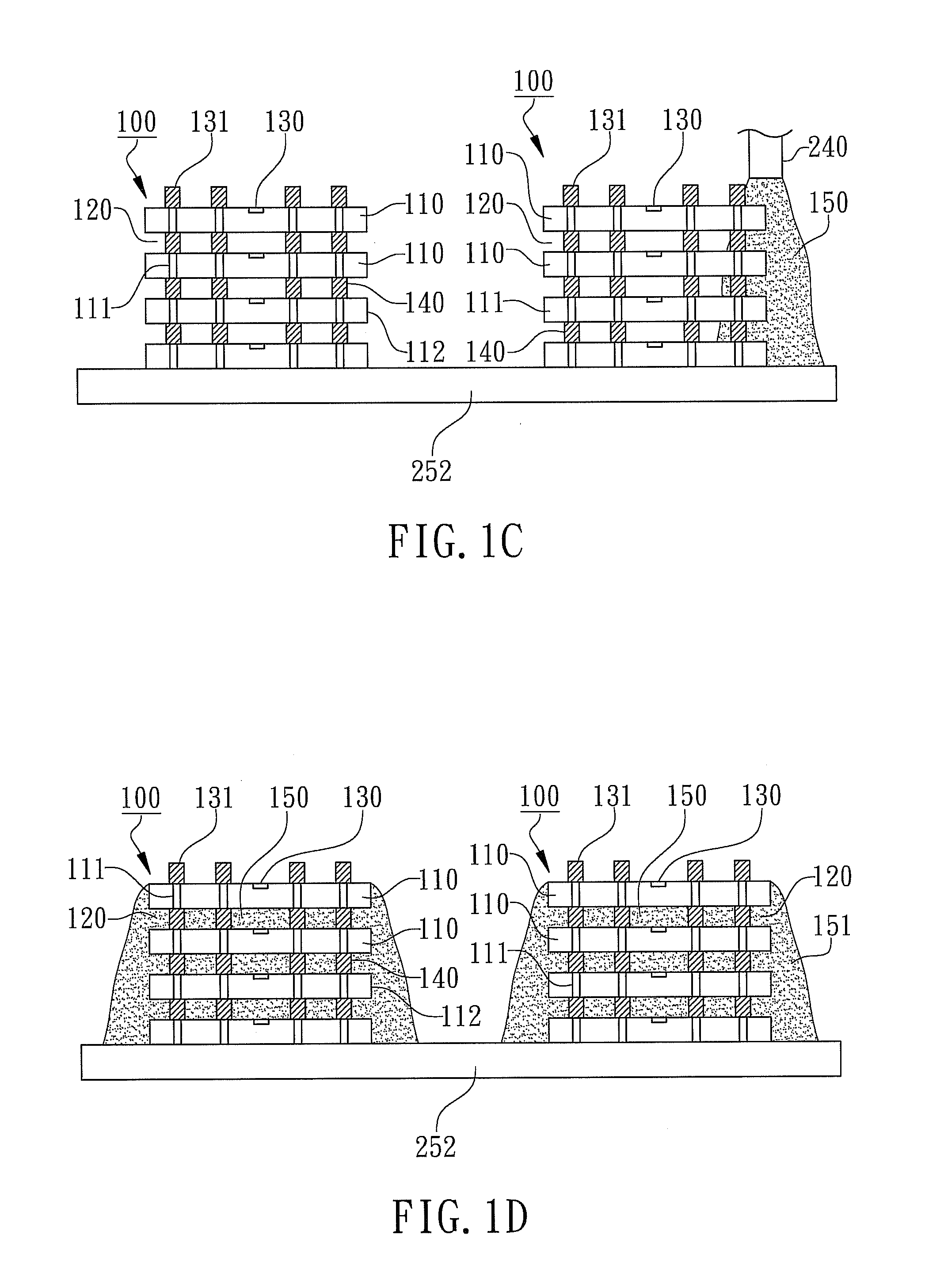
[0012]With reference to the attached drawings, the present invention is described by means of the embodiment(s) below where the attached drawings are simplified for illustration purposes only to illustrate the structures or methods of the present invention by describing the relationships between the components and assembly in the present invention. Therefore, the components shown in the figures are not expressed with the actual numbers, actual shapes, actual dimensions, nor with the actual ratio. Some of the dimensions or dimension ratios have been enlarged or simplified to provide a better illustration. The actual numbers, actual shapes, or actual dimension ratios can be selectively designed and disposed and the detail component layouts may be more complicated.

[0013]According to the preferred embodiment of the present invention, the method for testing multi-chip stacked packages is revealed where cross-sectional component views of each processing step of the method for testing mult...


PUM


Abstract

Disclosed is a method for testing multi-chip stacked packages. Initially, one or more substrate-less chip cubes are provided, each consisting of a plurality of chips such as chips stacked together having vertically connected with TSV's where there is a stacked gap between two adjacent chips. Next, the substrate-less chip cubes are adhered onto an adhesive tape where the adhesive tape is attached inside an opening of a tape carrier. Then, a filling encapsulant is formed on the adhesive tape to completely fill the chip stacked gaps. Next, the tape carrier is fixed on a wafer testing carrier in a manner to allow the substrate-less chip cubes to be loaded into a wafer tester without releasing from the adhesive tape. Accordingly, the probers of the wafer tester can be utilized to probe testing electrodes of the substrate-less chip cubes so that it is easy to integrate this testing method in TSV fabrication processes.

Description

FIELD OF THE INVENTION[0001]The present invention relates to a manufacture method of semiconductor devices, and more specifically to a method for testing multi-chip stacked packages.BACKGROUND OF THE INVENTION[0002]Multi-chip packaging is an advanced high-density packaging technology to vertically stacking a plurality of dice within the same package. The existing packaging method is to stack individual chips onto a substrate followed by corresponding packaging and testing processes. However, using a substrate increases overall package thickness and footprint.[0003]In order to reduce the dimension of a multi-chip package, there is an attempt to stack a plurality of chips using wafer-to-wafer bonding to manufacture a substrate-less chip cube such as related technology revealed in US Patent No. 2011 / 0074017. However, bad chips are always randomly present within a wafer, therefore, wafer-to-wafer bonding would cause overall packaging yield of substrate-less chip cubes to drop. Moreover,...

Claims


Application Information

Patent Timeline
Patent Type & Authority Applications(United States)
IPC IPC(8): G01R31/28
CPCG01R31/318513
Inventor CHANG, KAI-JUN
Owner POWERTECH TECHNOLOGY
Why Eureka
Try Eureka