Strained semiconductor-on-insulator (sSOI) by a simox method

a technology of strained semiconductors and on-insulators, applied in the direction of basic electric elements, electrical apparatus, semiconductor devices, etc., can solve the problems of reducing the manufacturability of substrates, reducing and affecting the quality of ssoi materials, so as to avoid wafer bonding and amorphization, and reduce the manufacturing cost of ssoi materials.

Active Publication Date: 2007-07-19
TAIWAN SEMICON MFG CO LTD
View PDF7 Cites 27 Cited by
  • Summary
  • Abstract
  • Description
  • Claims
  • Application Information

AI Technical Summary

Benefits of technology

[0009] One aspect of the present invention relates to methods for fabricating an sSOI material that overcome all of the drawbacks mentioned above with the prior art techniques of fabricating such materials. More particularly, the present invention provides methods of fabricating an sSOI material in which a single substrate and a separation by ion implantation of oxygen (SIMOX) process are used, thereby reducing the manufacturing cost of fabricating sSOI materials, while avoiding wafer bonding and amorphization.

Problems solved by technology

This prior method has an intrinsic complication because wafer bonding requires very smooth surfaces, and graded SiGe films typically have a very rough surface which makes graded SiGe films not suitable for use in most wafer bonding processes.
CMP is used in the prior art method to make the surfaces smoother, but CMP reduces the substrate manufacturability, especially for 300 mm wafers.
Moreover, the above method utilizes two expensive material technologies (i) epitaxial growth of a low-defect SiGe buffer layer and a strained Si layer, and (ii) layer transfer of the strain Si onto a handle substrate with an insulator.
The main drawbacks to the abovementioned concept are 1) the questionable ability to grow high-quality thick relaxed SiGe alloy layers with low-enough defect density, 2) the questionable ability to recrystallize through a very thick random alloy without generating new defects, 3) the practical challenge of amorphizing such a large buried region with a conventional implant procedure and 4) minimizing the interdiffusion of Ge into the lower Si layer during all these processing steps.
Despite being capable of forming an sSOI without wafer bonding or amorphization, this prior art technique requires separate regrowth steps to be performed after the SIMOX process that add additional processing steps and thus manufacturing costs in producing sSOI materials.

Method used


Image

  • Strained semiconductor-on-insulator (sSOI) by a simox method
  • Strained semiconductor-on-insulator (sSOI) by a simox method
  • Strained semiconductor-on-insulator (sSOI) by a simox method

Examples


Embodiment Construction

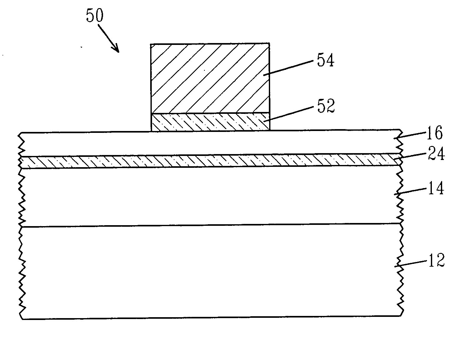
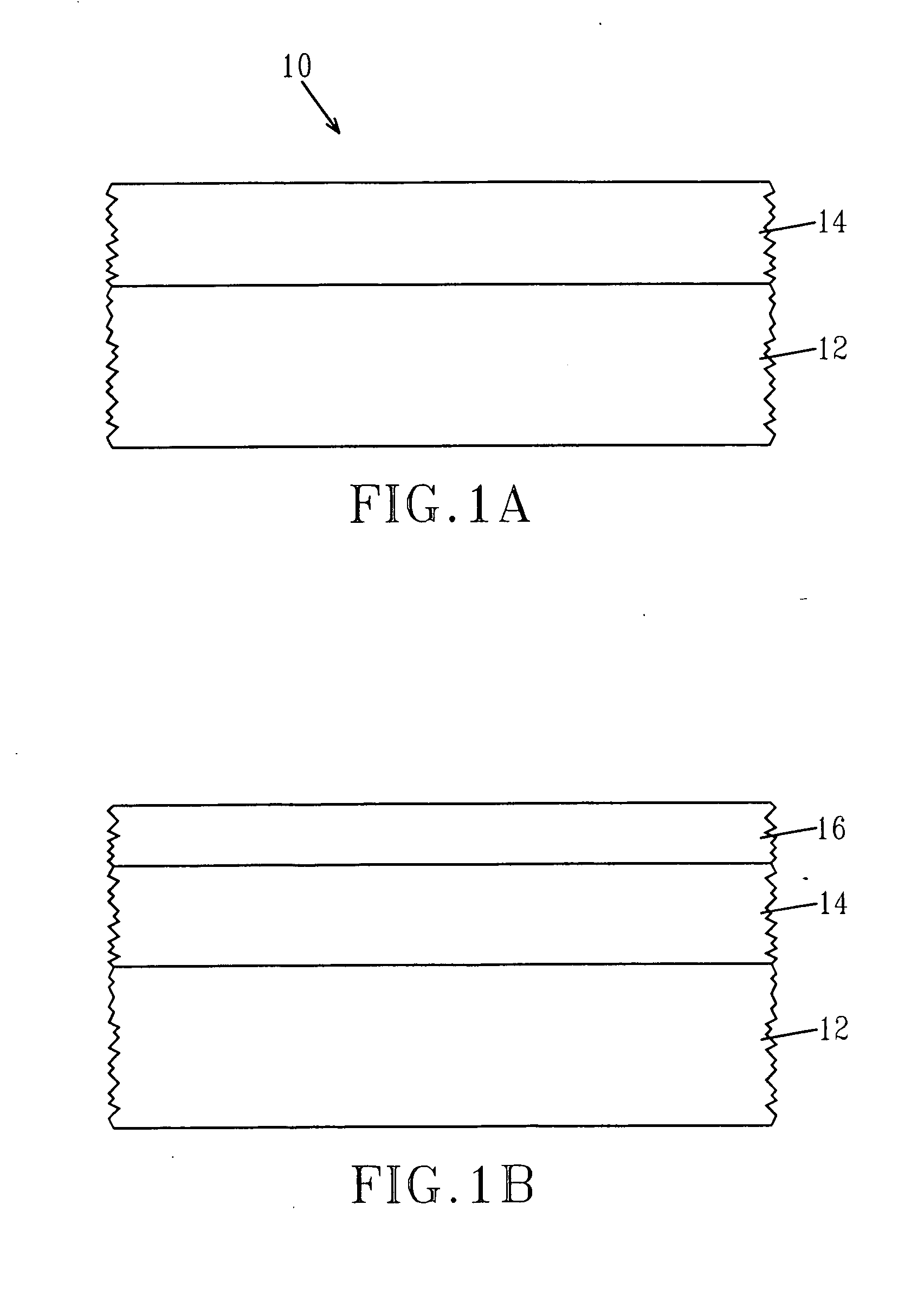
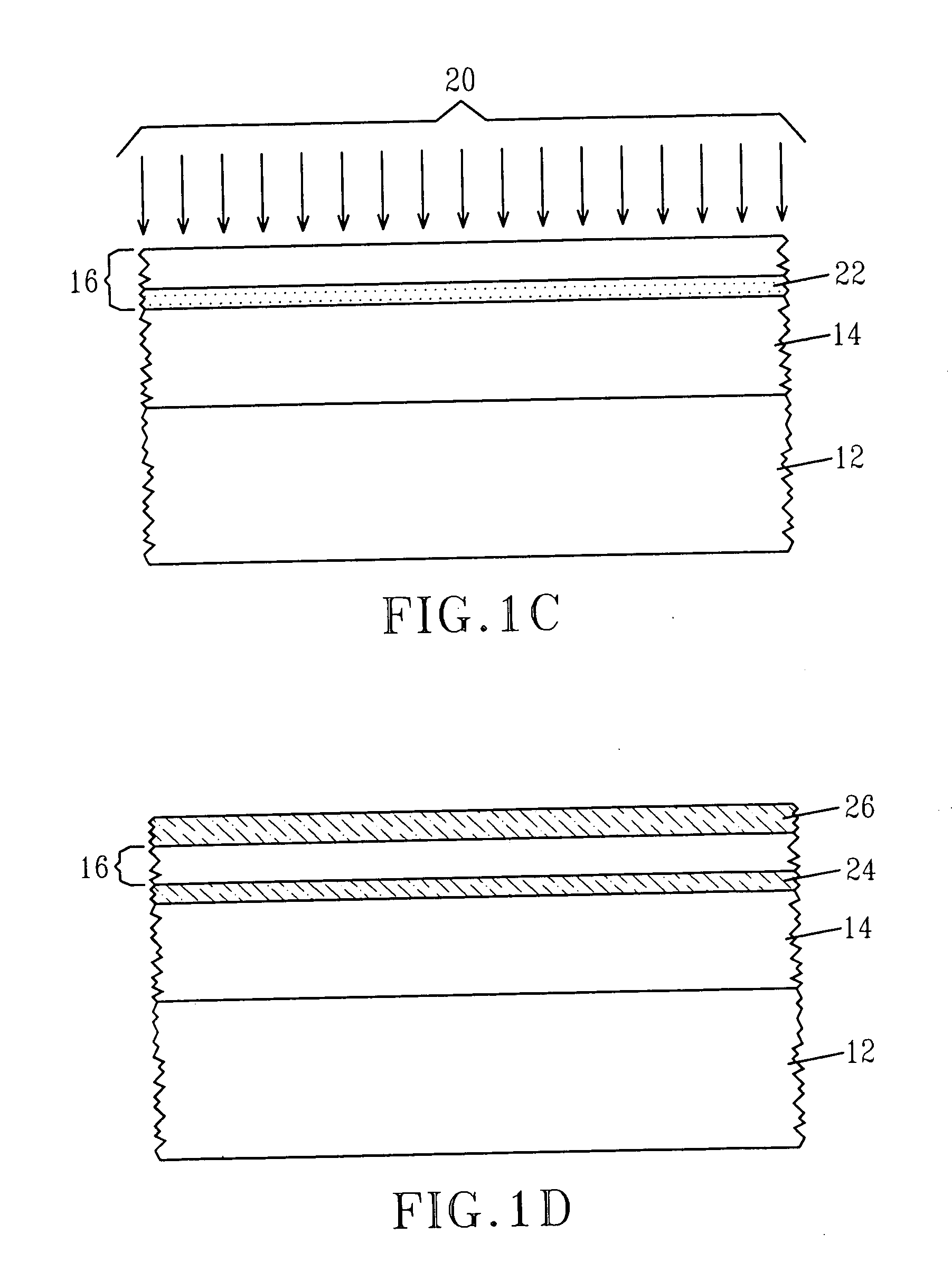
[0036] The present invention, which provides methods of fabricating strained semiconductor-on-insulator (sSOI) materials and the sSOI materials produced by the methods, will now be described in greater detail by referring to the drawings that accompany the present application. The drawings are provided for illustrative purposes only and, as such, they are not drawn to scale. In the drawings, like and corresponding elements are referred to by like reference numerals. It should be noted that throughout the present application the terms “layers” and “regions” can be interchangeable used.

[0037] As indicated above, the present invention provides a method of fabricating a tensile strained SOI material and a method of fabricating a compressive strained SOI material utilizing a single semiconductor wafer and a SIMOX process.

[0038] Reference is first made to FIGS. 1A-1E which are cross sectional views depicting the tensile strained SOI material of the present invention through various proc...


PUM


Abstract

A strained (tensile or compressive) semiconductor-on-insulator material is provided in which a single semiconductor wafer and a separation by ion implantation of oxygen process are used. The separation by ion implantation of oxygen process, which includes oxygen ion implantation and annealing creates, a buried oxide layer within the material that is located beneath the strained semiconductor layer. In some embodiments, a graded semiconductor buffer layer is located beneath the buried oxide layer, while in other a doped semiconductor layer including Si doped with at least one of B or C is located beneath the buried oxide layer.

Description

FIELD OF THE INVENTION [0001] The present invention relates to a method of fabricating a semiconductor structure, and more particularly to various methods of fabricating a strained semiconductor-on-insulator (sSOI) material. The present invention also relates to sSOI materials that are fabricated using the methods of the present invention. Both compressive strained and tensile strained materials are provided. BACKGROUND OF THE INVENTION [0002] Strained semiconductor-on-insulator structures for semiconductor devices combine the benefits of two advanced techniques for performance enhancement, namely, semiconductor-on-insulator (SOI) technology and strained semiconductor technology. On the one hand, a strained SOI configuration offers various advantages associated with the insulating substrate, such as reduced parasitic capacitances and improved isolation. On the other hand, strained semiconductors provide improved carrier mobilities. Devices such as strained semiconductor metal-oxide-...

Claims


Application Information

Patent Timeline
Patent Type & Authority Applications(United States)
IPC IPC(8): H01L27/12H01L21/84
CPCH01L21/76243H01L29/78654H01L29/7849H01L29/66772
Inventor ADAM, THOMAS N.BEDELL, STEPHEN W.DE SOUZA, JOEL P.FOGEL, KEITH E.REZNICEK, ALEXANDERSADANA, DEVENDRA K.SHAHIDI, GHAVAM
Owner TAIWAN SEMICON MFG CO LTD
Why Eureka
Try Eureka