Vertically formed inductor and electronic device having the same

a technology of inductance and electronic device, which is applied in the direction of inductance, continuous variable inductance/transformer, transformer/inductance coil/winding/connection, etc., can solve the problems of increasing manufacturing cost, increasing the size of the integrated circuit, and being unable to effectively increase the impedance, so as to minimize the loss of surface area and achieve high-efficiency impedance

Inactive Publication Date: 2008-12-04
ELECTRONICS & TELECOMM RES INST
View PDF12 Cites 65 Cited by
  • Summary
  • Abstract
  • Description
  • Claims
  • Application Information

AI Technical Summary

Benefits of technology

[0010]The present invention is directed to an inductor capable of minimizing a loss in surface area by the inductors by vertically disposing inductors on an electronic

Problems solved by technology

As a result, an increase in magnitude of the inductor causes an increase in size of the integrated circuit, thereby increasing manufacturing cost.
In addition, since it is needed to widen the surface area of the insulating layer in order to have desired impedance, it is impossible to effectively

Method used


Image

  • Vertically formed inductor and electronic device having the same
  • Vertically formed inductor and electronic device having the same
  • Vertically formed inductor and electronic device having the same

Examples


Embodiment Construction

[0021]The present invention will now be described more fully hereinafter with reference to the accompanying drawings, in which preferred embodiments of the invention are shown. This invention may, however, be embodied in different forms and should not be construed as limited to the embodiments set forth herein.

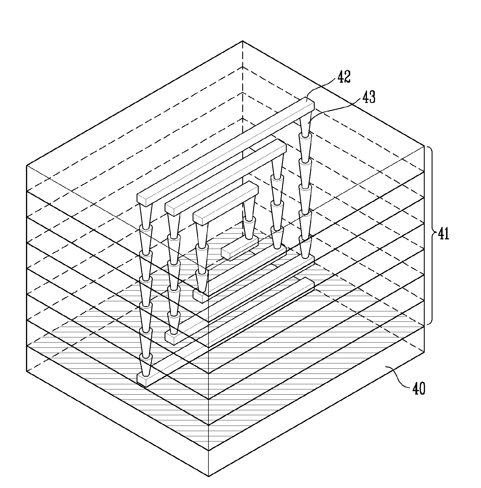
[0022]FIG. 4A is a schematic perspective view of an electronic device including a vertically formed spiral inductor in accordance with a first exemplary embodiment of the present invention, and FIG. 4B is a schematic side view of an electronic device including a vertically formed spiral inductor in accordance with the first exemplary embodiment of the present invention.

[0023]Referring to FIGS. 4A and 4B, the inductor in accordance with a first exemplary embodiment of the present invention is formed in a plurality of insulating layers (or dielectric layers) 41 formed on a substrate 40 and perpendicular to the substrate 40. It is difficult to form a conductive line pattern, whic...


PUM


Abstract

Provided are an inductor, which is vertically formed, and an electronic device having the inductor, and more particularly, an inductor capable of minimizing loss of a surface area and accomplishing high efficiency impedance by vertically forming the inductor in a plurality of insulating layers, and an electronic device having the same. The inductor includes a plurality of conductive lines disposed in the insulating layers; and vias vertically formed in the insulating layers to electrically connect the plurality of conductive lines. When a board or an electronic device including an inductor proposed by the present invention is manufactured, the inductor can occupy a minimum area in the electronic device or board while providing high inductance. In particular, the surface area of the electronic device or board occupied by the inductor can be remarkably decreased to reduce manufacturing costs.

Description

CROSS-REFERENCE TO RELATED APPLICATION[0001]This application claims the benefit of Korean Patent Application No. 2007-53172, filed May 31, 2007, and No. 2008-7736, filed Jan. 25, 2008, the disclosure of which is hereby incorporated herein by reference in its entirety.BACKGROUND[0002]1. Field of the Invention[0003]The present invention relates to a vertically formed inductor and an electronic device having the same, and more particularly, to an inductor capable of minimizing loss of a surface area and accomplishing high efficiency impedance by vertically forming the inductor on an insulating layer, and an electronic device having the same.[0004]2. Discussion of Related Art[0005]In recent times, with requirements of high integration of electronic components, a substrate, in which a plurality of layers are stacked, is generally used to perform a packaging process. The reason for performing the packaging process is that a larger number of active and passive components can be mounted on ...

Claims


Application Information

Patent Timeline
IPC IPC(8): H01F5/00
CPCH01F17/0013H01F17/0033H01F27/34H01F2017/002H01F2017/0073
Inventor YUN, HO GYEONGCHOI, KWANG SEONGMOON, JONG TAE
Owner ELECTRONICS & TELECOMM RES INST
Why Eureka
Try Eureka