Substrate with plane patterns and display device using the same

a technology of display device and plane pattern, which is applied in the association of printed circuit non-printed electric components, instruments, other domestic articles, etc., can solve problems such as abnormal patterns, and achieve the effect of reducing or preventing abnormal patterns

Active Publication Date: 2011-02-22
SHARP KK +1
View PDF25 Cites 1 Cited by
  • Summary
  • Abstract
  • Description
  • Claims
  • Application Information

AI Technical Summary

Benefits of technology

[0010]It is an object of the present invention to provide a substrate with high-precision plane patterns by which occurrence of an abnormal pattern is reduced or prevented in any pattern formed in a liquid process such as an inkjet method, and a display device using the substrate.
[0011]The present invention is characterized in that the plane patterns are formed based on a combination of plane shapes by which a difference in internal pressure of liquid ejected onto a substrate between any two points of the liquid is small, and the surface area of the liquid is reduced.
[0033]That is, a substrate with plane patterns formed using a liquid process according to the present invention is characterized in that the plane patterns are formed based on a combination of plane shapes by which a difference in internal pressure of liquid (solution of a pattern forming material) ejected onto a substrate so as to form the plane patterns is small between any two points of the liquid. The plane shapes are formed based on plane shapes by which the surface area of the liquid is minimized.
[0034]According to the present invention, in wiring patterns formed using a liquid process such as an inkjet method, the wiring patterns are formed by a combination of plane patterns by which the internal pressure of the liquid is constant in the plane patterns and the surface area of the liquid is minimized. Thus, it is possible to obtain a substrate in which occurrence of an abnormal pattern at the time of manufacturing is reduced or prevented. A display device (display panel) is constructed using the substrate having the plane patterns as wiring patterns. Thus, it is possible to obtain a low-cost and high-quality display device.

Problems solved by technology

The fact that the pattern has a shape different from a desired shape means that there occurs an abnormal pattern.

Method used


Image

  • Substrate with plane patterns and display device using the same
  • Substrate with plane patterns and display device using the same
  • Substrate with plane patterns and display device using the same

Examples


embodiment 1

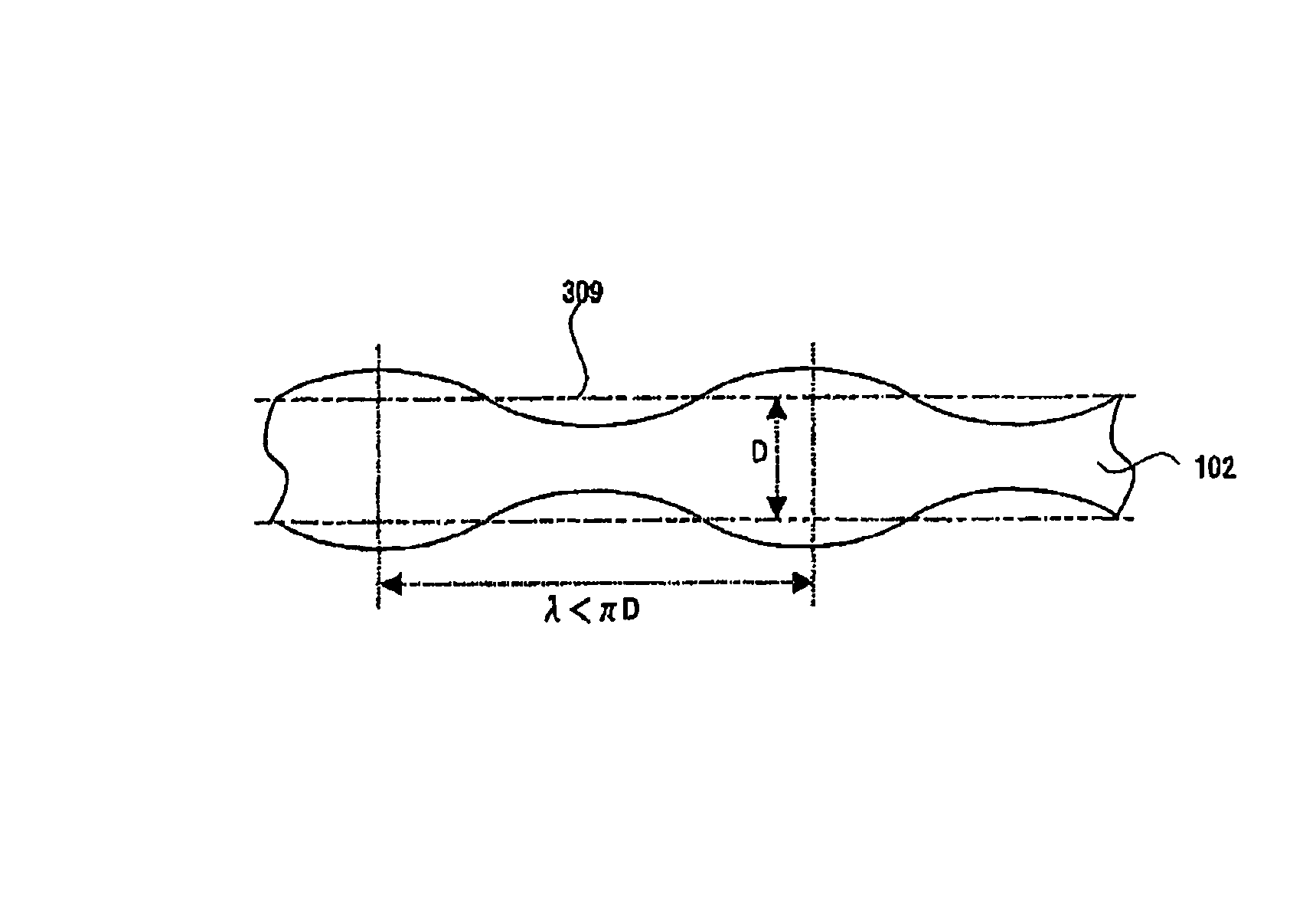
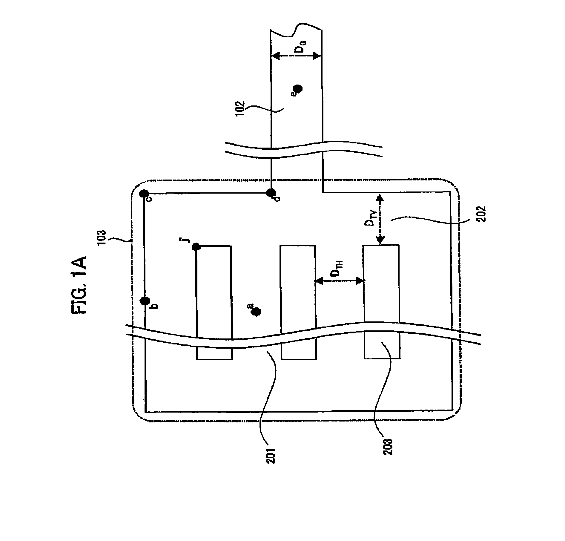
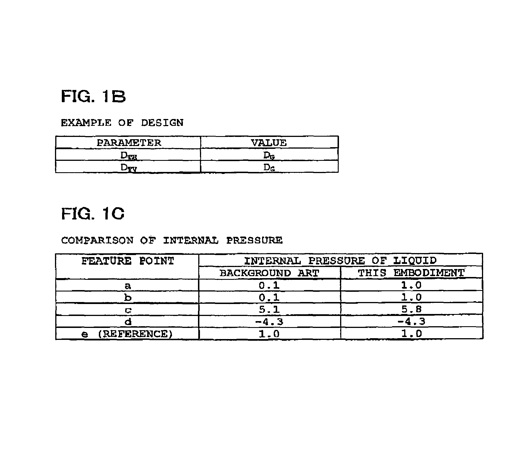
[0067]FIGS. 1A-1C are explanatory diagrams of Embodiment 1 of the present invention. FIG. 1A is a plan view showing a plane pattern of a terminal portion 103 formed in an inkjet method. FIG. 1B shows an example of design. FIG. 1C is a comparative table of internal pressure of liquid in feature points. A difference between internal pressure of liquid occurring at each feature point a, b of a terminal portion 103 and that at a feature point e of a scanning signal line 102 is caused by the width of the terminal portion 103 wider than the width of the scanning signal line 102.

[0068]In Embodiment 1, rod-like cut patterns 203 are disposed in the terminal portion 103 so as to form the terminal portion 103 into comb tooth patterns 201. A width DTH of each comb tooth pattern 201 is made equal to a width DG of the scanning signal line 102. The comb tooth patterns 201 are connected with one another through a comb teeth connection pattern 202 formed vertically. Like each comb tooth pattern 201,...

embodiment 2

[0073]FIGS. 2A-2C are explanatory diagrams of Embodiment 2 of the present invention. FIG. 2A is a plan view showing a plane pattern in a terminal portion 103 formed in an inkjet method. FIG. 2B shows an example of design. FIG. 2C is a comparative table of internal pressure of liquid in feature points. The chain line shows a background-art terminal portion plane pattern 301.

[0074]In Embodiment 2, circular cut patterns 204 are disposed on a square grille in the terminal portion 103. No pattern is formed in the region of each circular cut pattern 204. Thus, the terminal portion 103 is formed as a wiring pattern with circular holes made therein. The plane pattern is formed so that a radius rT of each terminal portion circular cut pattern 204 and an interval s between the terminal portion circular cut patterns 204 are 1.5DG and 0.8DG respectively with respect to a width DG of a scanning signal line 102.

[0075]The plane pattern according to Embodiment 2 improves the internal pressure of th...

embodiment 3

[0079]In Embodiment 3, chamfering 205 is applied to the inner side of the bent portion along a circle A of a radius rA around an origin O, and chamfering 206 is applied to the outer side of the bent portion along a circle B of a radius rB around the origin O. The plane pattern is formed so that the radius rA of the circle A is 2DG with respect to a width DG of the scanning signal line 102. The radius rB of the circle B is a sum of the radius rA of the circle A and the width DG of the scanning signal line 102. Thus, the radius rB of the circle B is 3DG.

[0080]Application of the plane pattern according to this embodiment improves the internal pressure of the liquid at the feature point c on a large scale so that the internal pressure of the liquid at the feature point c is 1.2 times as large as that at the feature point e, as compared with Embodiment 1 in which the former is 5.8 time as large as the latter. In the same manner, the internal pressure of the liquid at the feature point j′...


PUM

PropertyMeasurementUnit
contact angleaaaaaaaaaa

Abstract

A substrate with plane patterns formed in a liquid process wherein the plane patterns are formed based on a combination of plane shapes by which a difference in internal pressure of a solution between any two points of the solution is small, the solution being ejected onto the substrate so as to form the plane patterns by the liquid process.

Description

FIELD OF THE INVENTION[0001]The present invention relates to a substrate constituting a flat panel type display device and having plane patterns formed thereon, and a display device using the substrate, and particularly relates to a substrate in which plane patterns of scanning lines, video lines, source electrodes, semiconductor layers, pixel electrodes, etc. in a display panel constituting a flat panel type display device such as a liquid crystal display device or an organic EL display device are formed in a liquid process such as an inkjet method, and a display device using the substrate.BACKGROUND OF THE INVENTION[0002]For example, in a flat panel type display device such as a liquid crystal display device or an organic EL display device, a display panel constituting the display device has a display region in which a large number of pixels are arrayed in a matrix on a substrate. An active matrix display panel is used broadly as the display panel. In the active matrix display pan...

Claims


Application Information

Patent Timeline
Patent Type & Authority Patents(United States)
IPC IPC(8): B41M5/00
CPCG02F1/136286H05K3/125G02F2001/136295Y10S428/901H05K2203/013Y10T428/24802G02F1/136295G02F1/1343
Inventor ABE, MAKOTOKANEKO, HIROKITAKAHASHI, TAKUYANISHIMURA, ETSUKOTSUTSUI, YOSHITAKASUZUKI, TAKAAKI
Owner SHARP KK
Why Eureka
Try Eureka