Image sensor package and packaging method for the same

a technology of image sensor and packaging method, which is applied in the direction of radio frequency control devices, instruments, television systems, etc., can solve the problems of manufacturing errors still exist for the positioning portions, and the supporting member b>2/b> of solid-state image devices cannot be formed directly on the substrate, so as to improve the positioning accuracy of packaging, reduce the deviation between the sensing region of the sensor chip and the lens element, and improve the effect of positioning accuracy

Active Publication Date: 2008-12-11
ADVANCED SEMICON ENG INC
View PDF0 Cites 0 Cited by
  • Summary
  • Abstract
  • Description
  • Claims
  • Application Information

AI Technical Summary

Benefits of technology

[0011]In the image sensor package of the present invention, the lens central axis of the lens element carried by the frame is substantially coincided with the sensing region central axis of the sensor chip by forming at least one pair of guide pins inside the frame. Accordingly, the positional deviation between the sensing region of the sensor chip and the lens element can be decreased so as to improve the positioning accuracy in packaging.
[0012]According to the image sensor package of the present invention, the guide pins are formed integrally inside the frame by means of injection molding without increasing the manufacturing complexity.

Problems solved by technology

However, in an actual packaging process, manufacturing errors still exist for the positioning portions 4 of the solid-state image device 7 and the positioning portions 5 of the lens element 8.
However, the supporting member 2 of the solid-state image device cannot be formed directly on the substrate.

Method used


Image

  • Image sensor package and packaging method for the same
  • Image sensor package and packaging method for the same
  • Image sensor package and packaging method for the same

Examples


Embodiment Construction

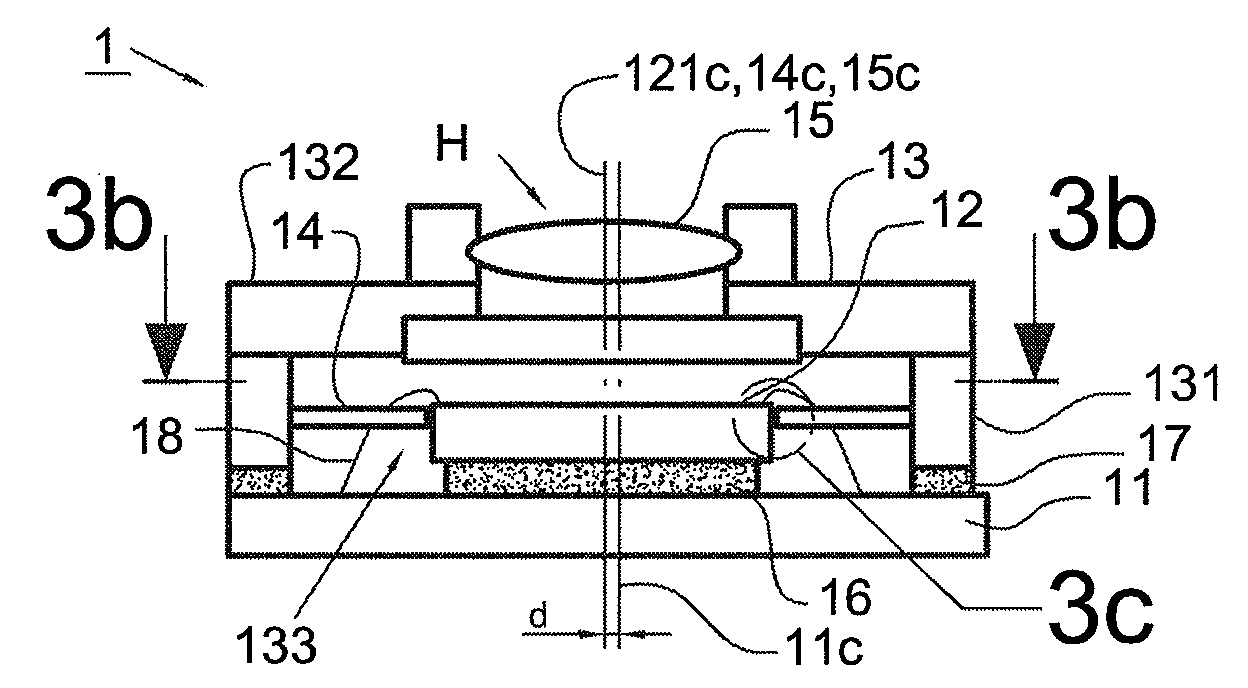
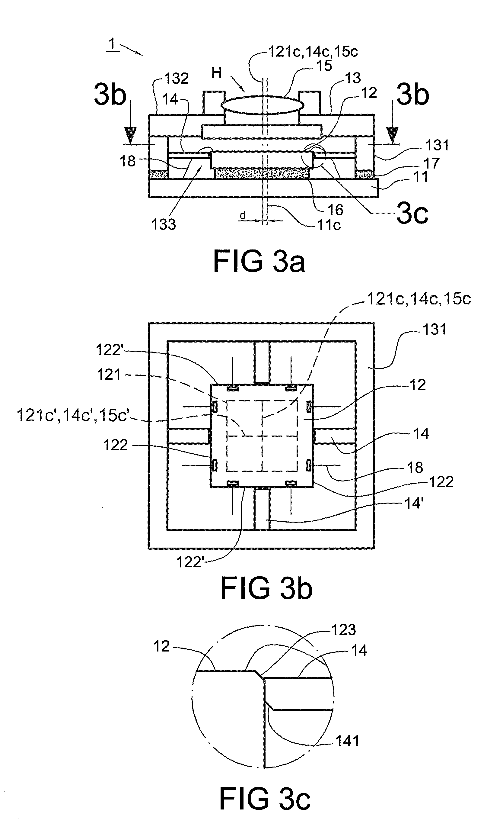
[0019]Referring to FIGS. 3a and 3b, FIG. 3a illustrates a sectional view of the image sensor package 1 according to one embodiment of the present invention and FIG. 3b shows a sectional view taken along the line 3b-3b of FIG. 3a. The image sensor package 1 includes a substrate 11, a sensor chip 12, a frame 13, at least a pair of first guide pins 14 and a lens element 15, and all these elements together form the image sensor package 1 of the present invention. Imaging beams are incident from outside of the image sensor package 1 to penetrate the lens element 15 and are then captured by an image sensing region 121 of the sensor chip 12.

[0020]Embodiments of the substrate 11 may be a printed circuit board or a ceramic circuit board, and the substrate 11 has a predetermined packaging line 11c served as a datum line for packaging the sensor chip 12 and the frame 13 thereon. Embodiments of the sensor chip 12 may be a Complementary Metal-Oxide-Semiconductor (CMOS) image sensing chip, a Char...


PUM


Abstract

An image sensor package includes a substrate, a sensor chip, a frame, a lens element and at least a pair of guide pins. The sensor chip is mounted on the substrate, and has two opposite sides and a sensing region, which has a sensing region central axis. The frame is mounted on the substrate, and has an aperture and an inner space with the sensor chip disposed therein. The lens element is disposed inside the aperture and has a lens central axis. The guide pins locate oppositely inside the inner space of the frame with an interval between the tips of the guide pins substantially identical to the distance between the opposite sides of the sensor chip, wherein the central line of the interval between the tips of the guide pins defines a positioning line, which substantially coincides with the lens central axis; wherein the tip of each guide pin is aligned with one of the opposite sides of the sensor chip such that the positioning line is substantially coincided with the sensing region central axis.

Description

CROSS REFERENCE TO RELATED APPLICATION[0001]This application claims the priority benefit of Taiwan Patent Application Serial Number 096120666, filed on Jun. 8, 2007, the full disclosure of which is incorporated herein by reference.BACKGROUND OF THE INVENTION[0002]1. Field of the Invention[0003]This invention generally relates to a semiconductor package and packaging method thereof, and more particularly, to an image sensor package and a packaging method for the same.[0004]2. Description of the Related Art[0005]In a conventional solid-state image device, as disclosed in Japanese patent publication number 61-134187 and entitled “Solid-State Image Pickup Device” as shown in FIG. 1, a CCD image sensing chip 303 is attached to a substrate 301 by means of an adhesive 302 and the substrate 301 has erected side walls 305 at its surroundings. A frame 307 for carrying a lens element 308 is fixed on the side walls 305 by means of an adhesive 306. However, in an actual packaging process, when t...

Claims


Application Information

Patent Timeline
Patent Type & Authority Applications(United States)
IPC IPC(8): H01L31/0203H01L31/18
CPCG02B7/02H01L27/14618H01L27/14625H04N5/2253H04N5/2254H04N5/2257H01L2224/45144H01L2224/48091H01L2924/00014H01L2924/00H04N23/54H04N23/50H04N23/57
Inventor CHEN, JIAN CHENG
Owner ADVANCED SEMICON ENG INC
Why Eureka
Try Eureka