Light-emitting apparatus

a technology of light-emitting apparatus and discharge tube, which is applied in the direction of discharge tube/lamp details, discharge tube luminescnet screen, organic semiconductor device, etc., can solve the problems of degrading the durability of the device, degrading the device characteristics and the device durability, and affecting so as to improve the efficiency of light extraction

Active Publication Date: 2008-12-11
CANON KK
View PDF12 Cites 73 Cited by
  • Summary
  • Abstract
  • Description
  • Claims
  • Application Information

AI Technical Summary

Benefits of technology

[0011]In view of the above-mentioned problems, an object of the present invention is to provide a light-emitting apparatus which can improve light extraction efficiency without adversely influencing a functional layer of a light-emitting device.
[0013]According to the present invention, the light extraction efficiency can be improved without adversely influencing the functional layer of the light-emitting device.

Problems solved by technology

According to the technologies disclosed in U.S. Pat. No. 5,779,924 and Japanese Patent Application Laid-Open No. 2004-349111 above, in the case of disposing a periodic structure at an upper portion of a functional layer, it is necessary to make the periodic structure after formation of the functional layer, so that there is a problem that the functional layer may be damaged during the making process of the periodic structure.
Further, in the case of disposing a periodic structure at a lower portion of a functional layer, because the interface between the functional layer and an electrode, or the like is not flat, there is a problem that non-uniformity and reduction in adhesiveness of a film and the like occur during formation of the film by vacuum vapor deposition, which may degrade the device characteristics and the device durability.
Therefore, there is a problem of degradation of the device durability caused by local light emission and increase of the number of non-light-emitting devices due to short-circuiting between the electrodes.

Method used


Image

  • Light-emitting apparatus
  • Light-emitting apparatus
  • Light-emitting apparatus

Examples


example 1

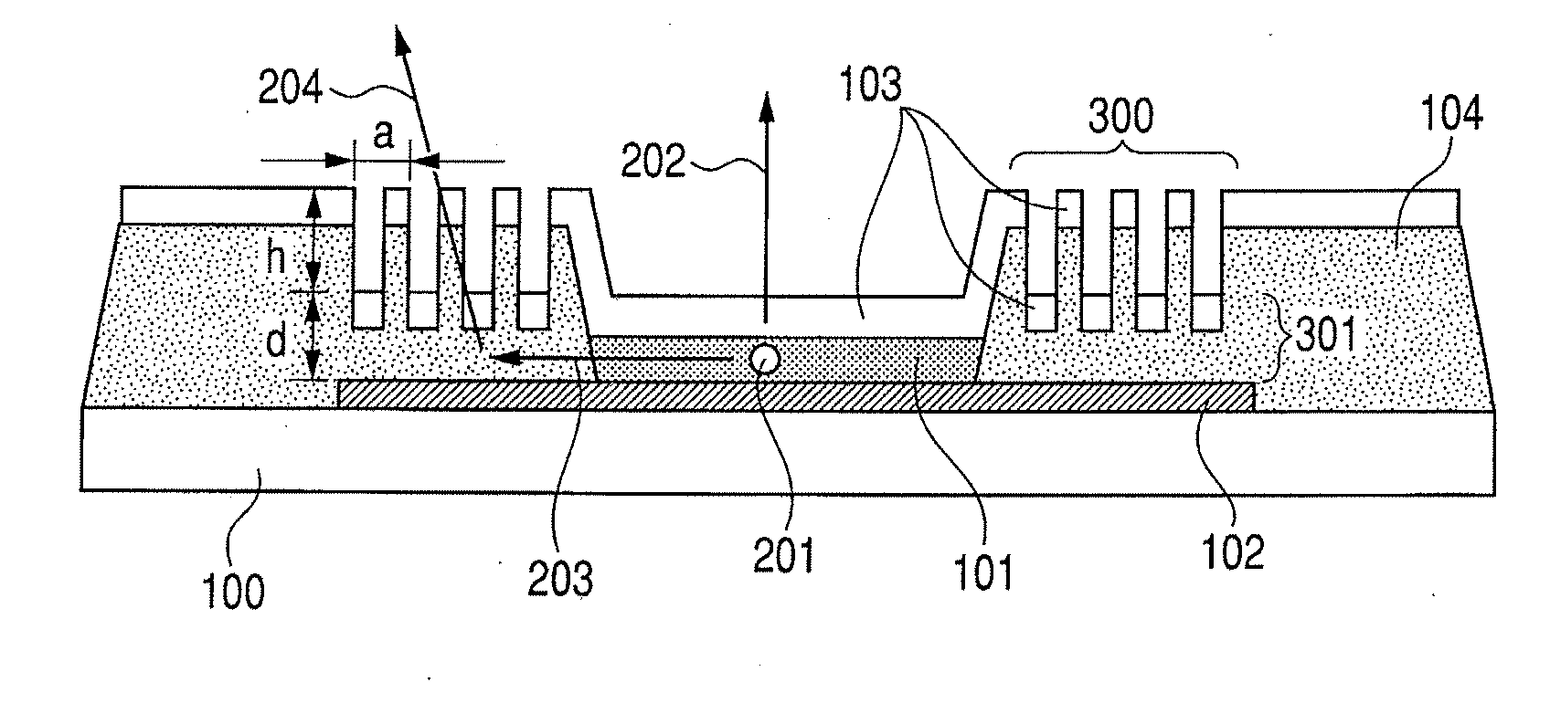
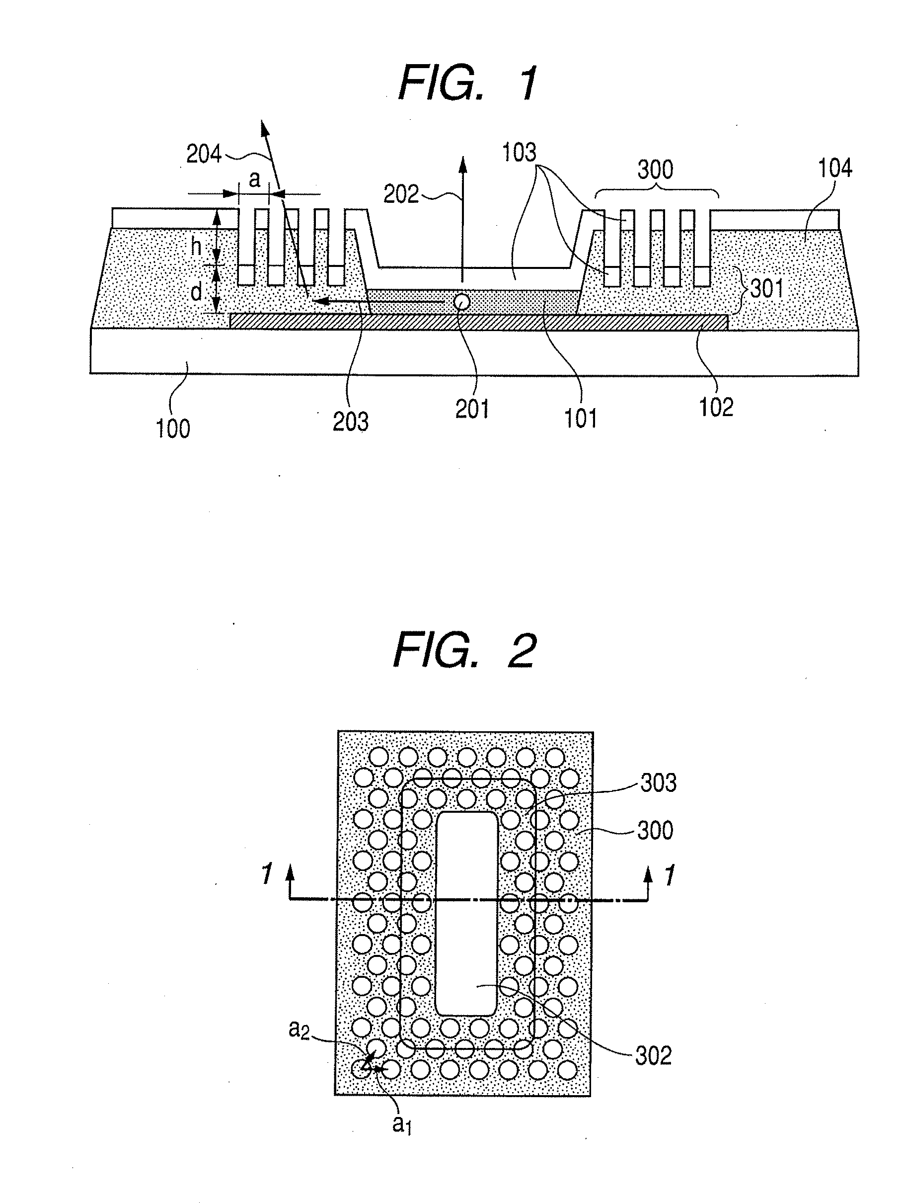
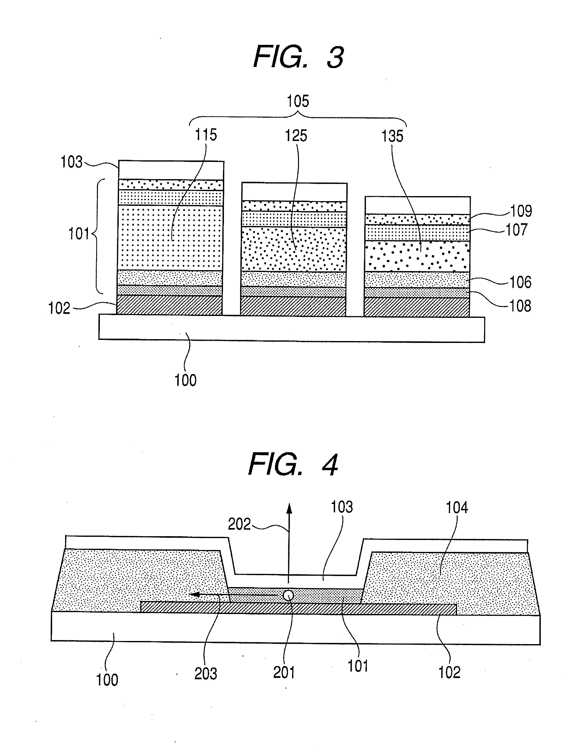
[0106]A full-color organic light-emitting apparatus of a structure illustrated in FIG. 13 is produced by the method described below. More specifically, the light-emitting apparatus of this example is an organic light-emitting apparatus having a plurality of pixels, each pixel being composed of a red-light-emitting device, a green-light-emitting device, and a blue-light-emitting device (i.e., sub-pixels of three colors of red, green, and blue), and can be applied preferably as a display apparatus. Hereinafter, the red-light-emitting device is referred to as an R device, the green-light-emitting device is referred to as a G device, and the blue-light-emitting device is referred to as a B device.

[0107]First, a TFT driving circuit made of low-temperature polysilicon is formed on a glass substrate 100 as a support member, and a planarizing film made of an acrylic resin is formed on the TFT driving circuit to obtain a substrate. A film of an Ag alloy (AgPdCu) as a reflective metal is form...

example 2

[0117]FIG. 14 is a structural view of an organic EL light-emitting apparatus of Example 2. The production process of Example 2 is the same as Example 1 before the formation of the hole-transporting layer. In each sub-pixel, a film of Compound (I) above is formed as a hole-transporting layer of an R device in a thickness of 70 nm, as a hole-transporting layer of a G device in a thickness of 40 nm, and as a hole-transporting layer of a B device in a thickness of 20 nm, respectively. Next, as a common 3-color stack type white (W) emission layer, CBP and bis[(4,6-difluorophenyl)pyridinato-N,C2] (picolinato)Iridium (hereinafter, referred to as FIrpic) are co-deposited in a thickness of 25 nm. Then, CBP and Btp2Ir(acac) (weight ratio 92:8) are co-deposited in a thickness of 2 nm. Further, CBP and bis(2-phenylbenzothiozolato-N—C2)Iridium(acetylacetonate) (hereinafter, referred to as Bt2Ir(acac) (weight ratio is 92:8) are co-deposited in a thickness of 2 nm, thereby obtaining a stack struct...

example 3

[0119]FIG. 15 is a structural view of an organic light-emitting apparatus of Example 3. The process for the formation of the layers up to and including the electron injection layer is the same as that of Example 1. The substrate having the layers up to and including the electron injection layer formed thereon is moved to a sputtering apparatus without breaking the vacuum, and a film of an Ag alloy is formed to have a thickness of 20 nm as a metal semi-transparent electrode 193.

[0120]Further, a desiccant is disposed at the periphery of the light-emitting apparatus, and the apparatus is sealed with etched cap glass, whereby an organic light-emitting apparatus is obtained.

[0121]More specifically, the organic light-emitting apparatus of this example has a structure in which an organic layer 111 of an R device, an organic layer 121 of a G device, and an organic layer 131 of a B device are formed in each sub-pixel, and has a metal semi-transparent electrode.


PUM


Abstract

Provided is a light-emitting apparatus which can improve the light extraction efficiency without adversely influencing a functional layer of a light-emitting device and which includes a substrate; a light-emitting device formed on the substrate, the light-emitting device including: a first electrode formed on the substrate; an insulating member covering a periphery of the first electrode; and a functional layer formed on an exposed portion of the first electrode and including an emission layer; and a second electrode formed on the functional layer and the insulating member, in which a periodic structure is formed on a surface of the insulating member opposite to a substrate side, and an optical waveguide is formed between a bottom portion of the periodic structure and the first electrode or between the bottom portion of the periodic structure and the substrate.

Description

BACKGROUND OF THE INVENTION[0001]1. Field of the Invention[0002]The present invention relates to a light-emitting apparatus.[0003]2. Description of the Related Art[0004]An organic electroluminescent (EL) display, being a kind of light-emitting apparatus, is a new type of flat panel display and formed from an array of organic light-emitting diode (OLED) devices. In general, an OLED device is comprised of an electrode serving as the anode, an electrode serving as the cathode and several thin organic layers sandwiched between these two electrodes. The organic layers include at least one emission layer containing more than one fluorescent or phosphorescent organic compounds to emit light of each emission color. When applying a voltage to the OLED device, holes and electrons are injected from the anode and the cathode, respectively, and form excitons in the emission layer. Then these excitons recombine and release their energy as emission of light. According to a research conducted by Ea...

Claims


Application Information

Patent Timeline
Patent Type & Authority Applications(United States)
IPC IPC(8): H01J1/62
CPCH01L27/3246H01L33/44H01L33/54H01L51/0081H01L51/0085H01L51/5262H01L51/5265H01L51/5268H01L2251/5315H10K59/122H10K85/324H10K85/342H10K50/85H10K50/852H10K50/854H10K2102/3026
Inventor FUKUDA, KOICHI
Owner CANON KK
Why Eureka
Try Eureka