Pattern forming method using relacs process

a technology of relacs and pattern forming, which is applied in the direction of photomechanical treatment, instruments, photomechanical apparatus, etc., can solve the problem of difficult to remove resis

Inactive Publication Date: 2008-12-11
KK TOSHIBA
View PDF10 Cites 382 Cited by
  • Summary
  • Abstract
  • Description
  • Claims
  • Application Information

AI Technical Summary

Benefits of technology

[0009]FIGS. 1A to 1H are sectional views showing the steps in a conventional pattern forming method using a spacer process;

Problems solved by technology

This makes it difficult to remove the resist.

Method used


Image

  • Pattern forming method using relacs process
  • Pattern forming method using relacs process
  • Pattern forming method using relacs process

Examples


first embodiment

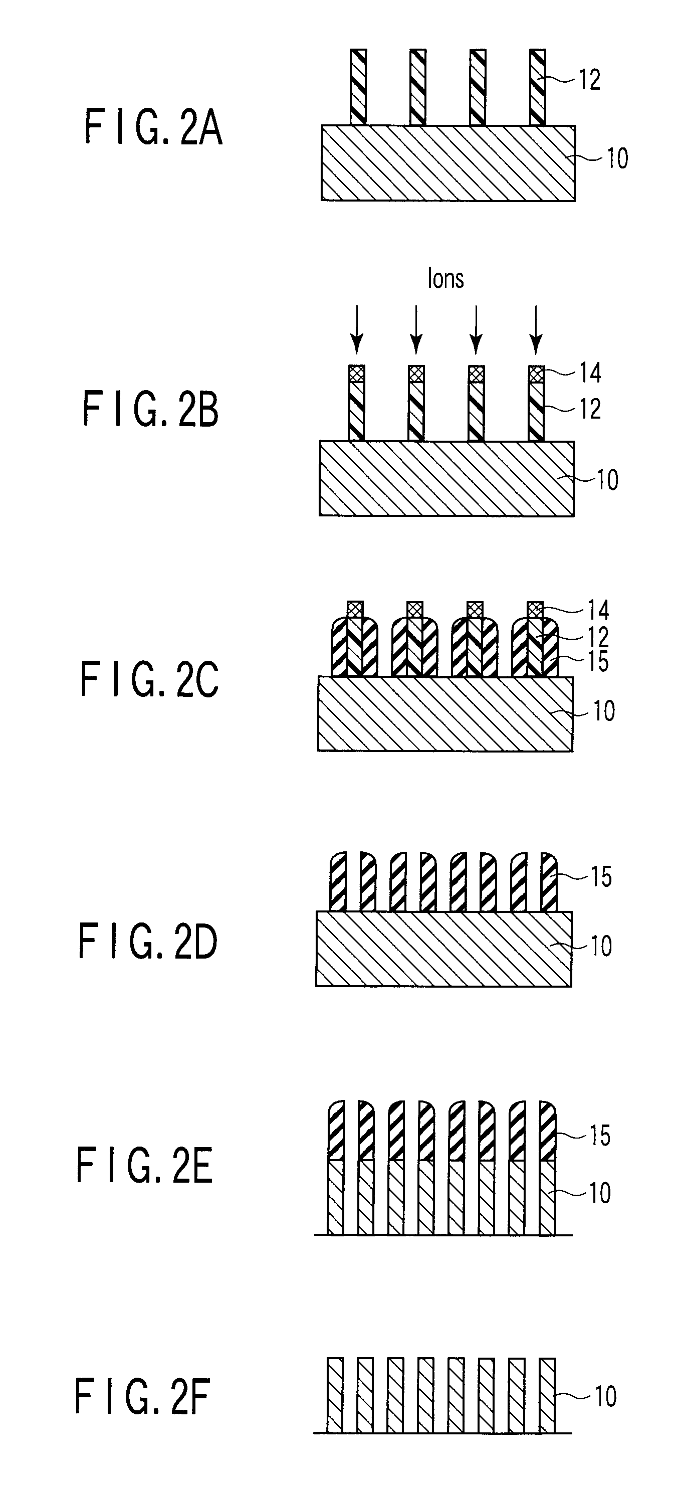
[0014]A pattern forming method according to the first embodiment of the present invention will be described with reference to FIGS. 2A to 2F.

[0015]In this embodiment, a sidewall pattern is formed using RELACS. Additionally, ions are implanted in advance to prevent a RELACS film from remaining on the upper surface of a resist pattern, thereby deactivating the acid in the resist.

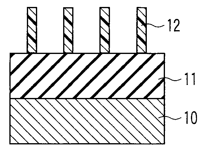
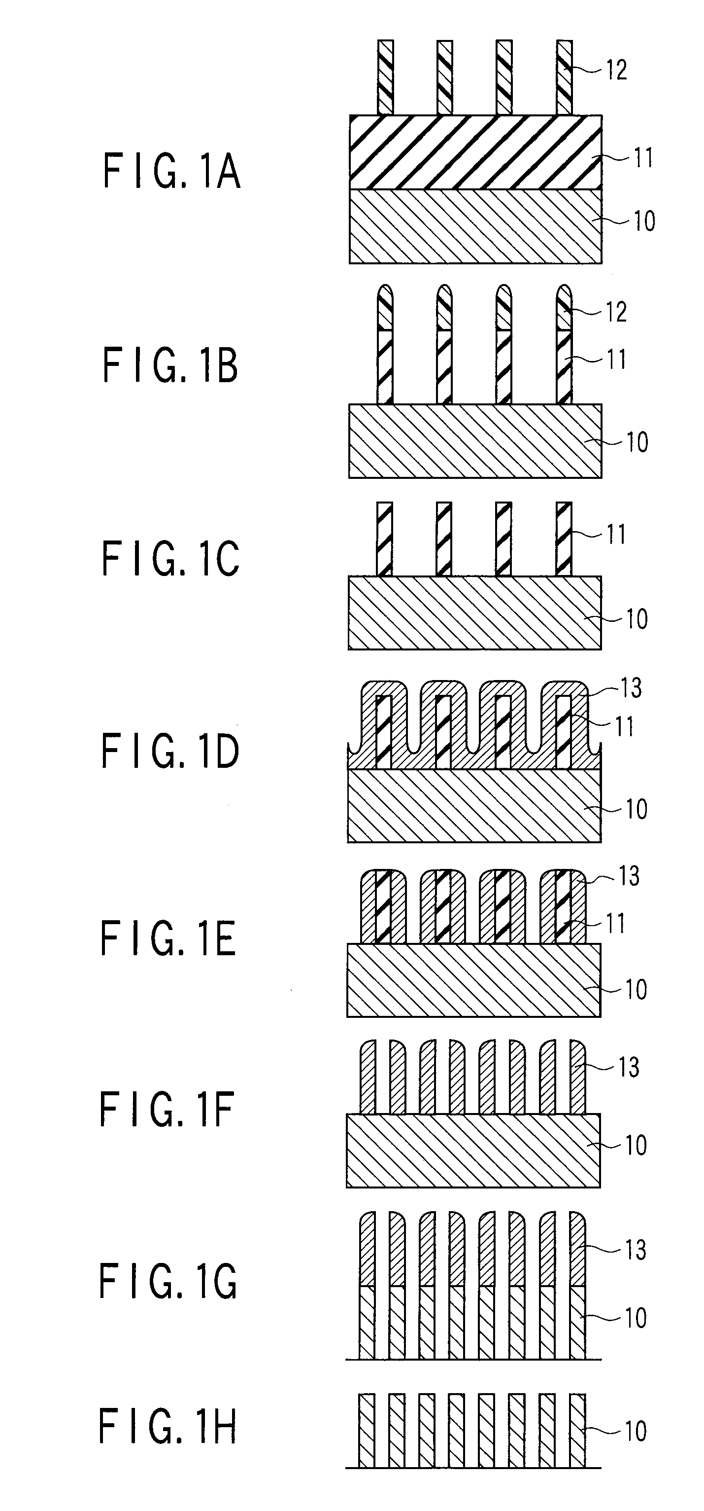
[0016]As a comparison to this embodiment, a conventional spacer process will be described first with reference to FIGS. 1A to 1H. In the conventional spacer process, as shown in FIG. 1A, an oxide film 11 such as a TEOS film is formed on a to-be-processed film 10 made of, e.g., silicon (Si), polysilicon (poly-Si), an oxide film, or tungsten (W). A resist pattern 12 is formed on the oxide film 11.

[0017]At this time, a desired resist pattern 12 may directly be formed by exposure. Alternatively, the resist pattern 12 may be formed by slimming. In this case, a resist pattern 12, of which line width is wider than th...

second embodiment

[0059]A pattern forming method according to the second embodiment of the present invention will be described with reference to FIGS. 2A to 2F and FIGS. 5A to 5F.

[0060]In the first embodiment, the explanation has been made assuming that only a cell portion is formed. However, if the cell portion and the peripheral circuit portion are formed separately, the manufacturing cost increases. In the second embodiment, a method of forming the peripheral circuit portion and the cell portion simultaneously will be described. It is therefore possible to execute the following steps of forming the peripheral circuit portion simultaneously in parallel to the steps described in the first embodiment.

[0061]FIGS. 5A to 5F are sectional views showing the steps in manufacturing a peripheral circuit portion. The steps in FIGS. 5A to 5F correspond to the steps in FIGS. 2A to 2F, respectively. The corresponding steps are executed simultaneously.

[0062]As shown in FIG. SA, in the first resist patterning step...


PUM

PropertyMeasurementUnit
thicknessaaaaaaaaaa
vapor pressureaaaaaaaaaa
solvent resistanceaaaaaaaaaa

Abstract

A resist pattern is formed on a to-be-processed film. Ions are implanted in the upper surface of the resist pattern. After ion implantation, an organic film is formed to cover the resist pattern and heated. A crosslinked resin film made of the organic film which has crosslinked is formed on the sidewall of the resist pattern by developing the organic film after heating. After formation of the crosslinked resin film, the resist pattern is removed. The to-be-processed film is processed using the crosslinked resin film as a mask.

Description

CROSS-REFERENCE TO RELATED APPLICATIONS[0001]This application is based upon and claims the benefit of priority from prior Japanese Patent Application No. 2007-154484, filed Jun. 11, 2007, the entire contents of which are incorporated herein by reference.BACKGROUND OF THE INVENTION[0002]1. Field of the Invention[0003]The present invention relates to a lithography technique of forming a semiconductor device pattern and, more particularly, to a pattern forming method of forming a pattern with double the frequency of a resist pattern using a RELACS process.[0004]2. Description of the Related Art[0005]There is a growing need for micropatterning of semiconductor devices, although the wavelength of exposure light in an exposure apparatus shortens, and the NA (Numerical Aperture) increases. To meet this requirement, pattern forming methods of doubling the frequency (or halving the pitch) have been proposed and examined. One of the methods of forming a pattern which doubles the frequency is ...

Claims


Application Information

Patent Timeline
Patent Type & Authority Applications(United States)
IPC IPC(8): G03F7/004
CPCH01L21/0273H01L21/3086H01L21/3088H01L21/31144H01L21/32139
Inventor NAKAMURA, HIROKO
Owner KK TOSHIBA
Why Eureka
Try Eureka