

Gas supply mechanism and substrate processing apparatus
a technology of gas supply mechanism and substrate, which is applied in the direction of electric discharge tubes, coatings, chemical vapor deposition coatings, etc., can solve the problems of film formation rate or etching, inability to achieve desired processing results, and inability to process longer, etc., to achieve the effect of leaking easily into the gap
- Summary
- Abstract
- Description
- Claims
- Application Information
AI Technical Summary
Benefits of technology
Problems solved by technology
Method used
Image

Examples
first embodiment
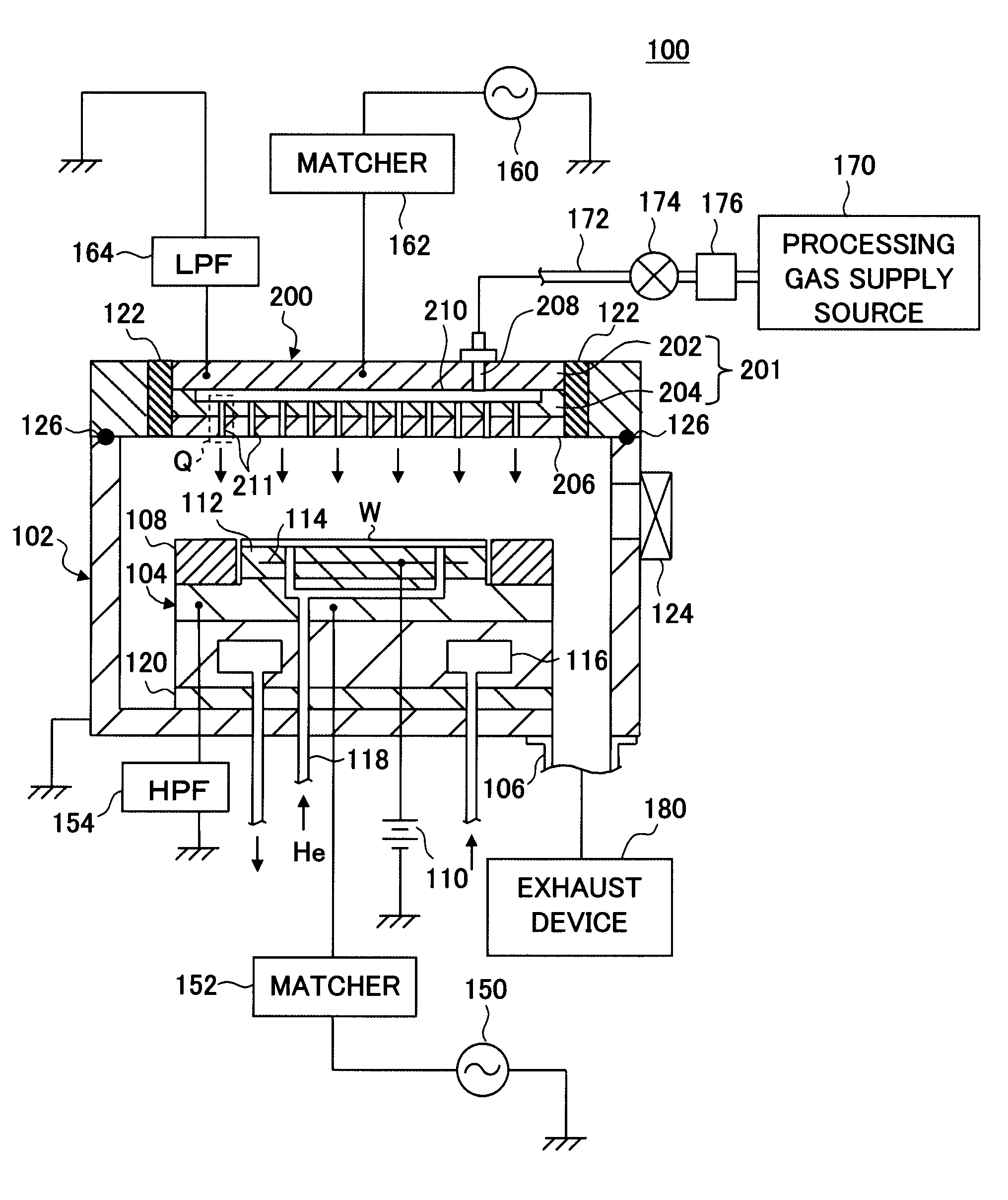
[0045]A substrate processing apparatus that may adopt the processing gas supply mechanism achieved in the present invention is now described. The explanation is given by assuming that the substrate processing apparatus is a plane-parallel plasma processing apparatus having an upper electrode and a lower electrode (susceptor) disposed to face opposite each other inside a processing chamber with a processing gas supplied into the processing chamber through the upper electrode and that the processing gas supply mechanism according to the present invention is adopted in the upper electrode. FIG. 1 schematically illustrates the structure of the plasma processing apparatus achieved in the embodiment in a sectional view. It is to be noted that in order to simplify the illustration, FIG. 1 shows a smaller number of processing gas supply holes 211 than the number of processing gas supply holes that are actually formed.
[0046]The plasma processing apparatus 100 includes a processing chamber 10...
second embodiment
[0090](Processing Gas Supply Holes Achieved in the Second Embodiment)
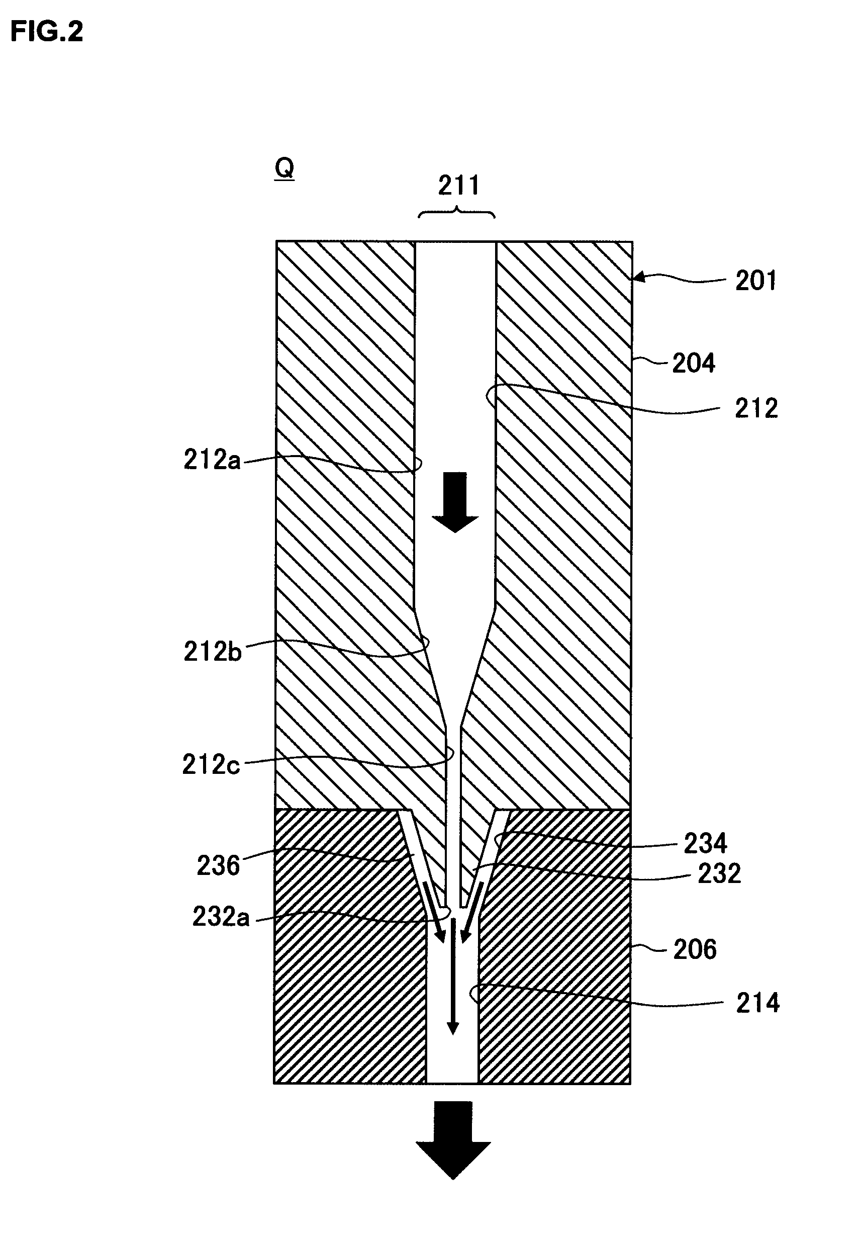
[0091]Next, the processing gas supply holes achieved in the second embodiment of the present invention are described in reference to a drawing. FIG. 4 illustrates the structure adopted in the processing gas supply holes in the embodiment, in an enlargement of an area Q over which one of processing gas supply holes in FIG. 1 is formed. The processing gas supply holes 211 in the second embodiment are each formed by layering a plate-like middle member 205 constituted of a material that inhibits heat input and an abnormal electrical discharge attributable to plasma and heat radiation, between the processing gas supply mechanism main unit 201 and the electrode plate 206 shown in FIG. 3, with nozzle portions 232 formed at the middle member 205. It is to be noted that in FIG. 4, the same reference numerals are assigned to parts having functions similar to those in FIG. 3 so as to preclude the necessity for a detailed expl...
PUM
| Property | Measurement | Unit |
|---|---|---|
| frequency | aaaaa | aaaaa |
| frequency | aaaaa | aaaaa |
| coefficient of thermal expansion | aaaaa | aaaaa |
Abstract
Description
Claims
Application Information