
Semiconductor device and method for manufacturing semiconductor device

a semiconductor and semiconductor technology, applied in the direction of semiconductor devices, basic electric elements, electrical equipment, etc., can solve the problems of difficult to introduce dopants using the conventional ion implantation method, more expensive soi wafers than the conventional method, and self-heating effect, so as to prevent the diffusion of ionic species, increase the on current, and shorten the channel length

Inactive Publication Date: 2008-12-25
ELPIDA MEMORY INC
View PDF3 Cites 23 Cited by
  • Summary
  • Abstract
  • Description
  • Claims
  • Application Information

AI Technical Summary

Benefits of technology

"The invention provides a semiconductor device and a method for manufacturing it that can realize an extremely short channel length without changing the threshold value. This is achieved by forming a spiral body in a protrudent form with a linear semiconductor layer on which a body region including a channel region and a first source / drain region is formed, and a gate insulating film and a gate electrode that are opposed to the pair of sidewall portions of the linear semiconductor layer. The semiconductor device includes a semiconductor substrate, a spiral body, a first source / drain region, a second source / drain region, and a lead-out electrode. The method for manufacturing the semiconductor device includes sequentially forming a first semiconductor film, a second semiconductor film, and a third semiconductor film to form the linear semiconductor layer in a protrudent form. The linear semiconductor layer has a pair of sidewall portions and a gate insulating film covering the sidewall portions. The method also includes patterning the substrate surface to form a linear semiconductor layer and a lead-out electrode. The semiconductor device and method can realize a small size and high integration LSI circuit. Additionally, the method can suppress the short channel effect and the short channel effect can be further suppressed by the use of the spiral structure and the introduction of the gate insulating film."

Problems solved by technology

However, the SOI wafers are more expensive than the conventional single-crystalline silicon wafers, and therefore, there is a desire to provide a transistor having characteristics equivalent to the SOI-CMOS transistor by using the conventional single-crystalline silicon wafers.
In addition, the SOI wafers have a drawback in that the thermal conductivity of the buried oxide film differs greatly from that of the silicon layer, which causes the self-heating effect.
However, when the transistor is manufactured with such a structure, it is difficult to introduce dopants using the conventional ion implantation method.
However, as the requirements for the higher integration density become stricter, the gate length will decrease year after year, and it is thus thought that it will ultimately reach the limit within 20 years in future.
However, when the channel is formed in the body region, it is difficult to practically control the current in the small gate region and thus the short channel effect occurs.
However, the planar type transistor with an all-around gate requires a complex manufacturing process.
For this reason, the FinFET is disadvantageous in terms of integration with a conventional planar transistor, usability as a substitute, and area efficiency.
Therefore, it is disadvantageous for realization of an extremely short channel length.
Moreover, since the transistor is shaped to extend in a direction perpendicular to or parallel to the substrate, the transistor has an unbalanced shape that does not exhibit the inherent characteristics of the FinFET.
Therefore, there is a problem in that the manufacturing the transistor is practically impossible.

Method used


Image

  • Semiconductor device and method for manufacturing semiconductor device
  • Semiconductor device and method for manufacturing semiconductor device
  • Semiconductor device and method for manufacturing semiconductor device

Examples


Embodiment Construction

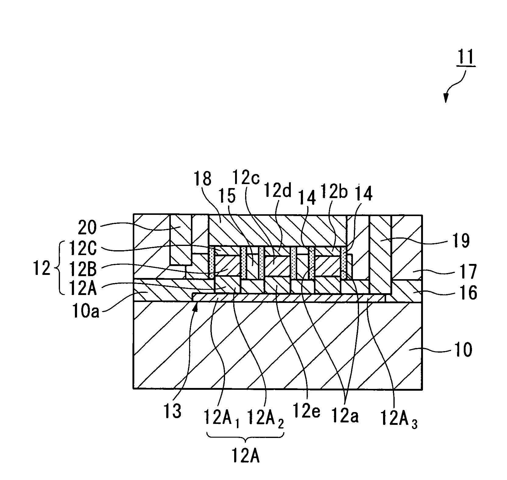
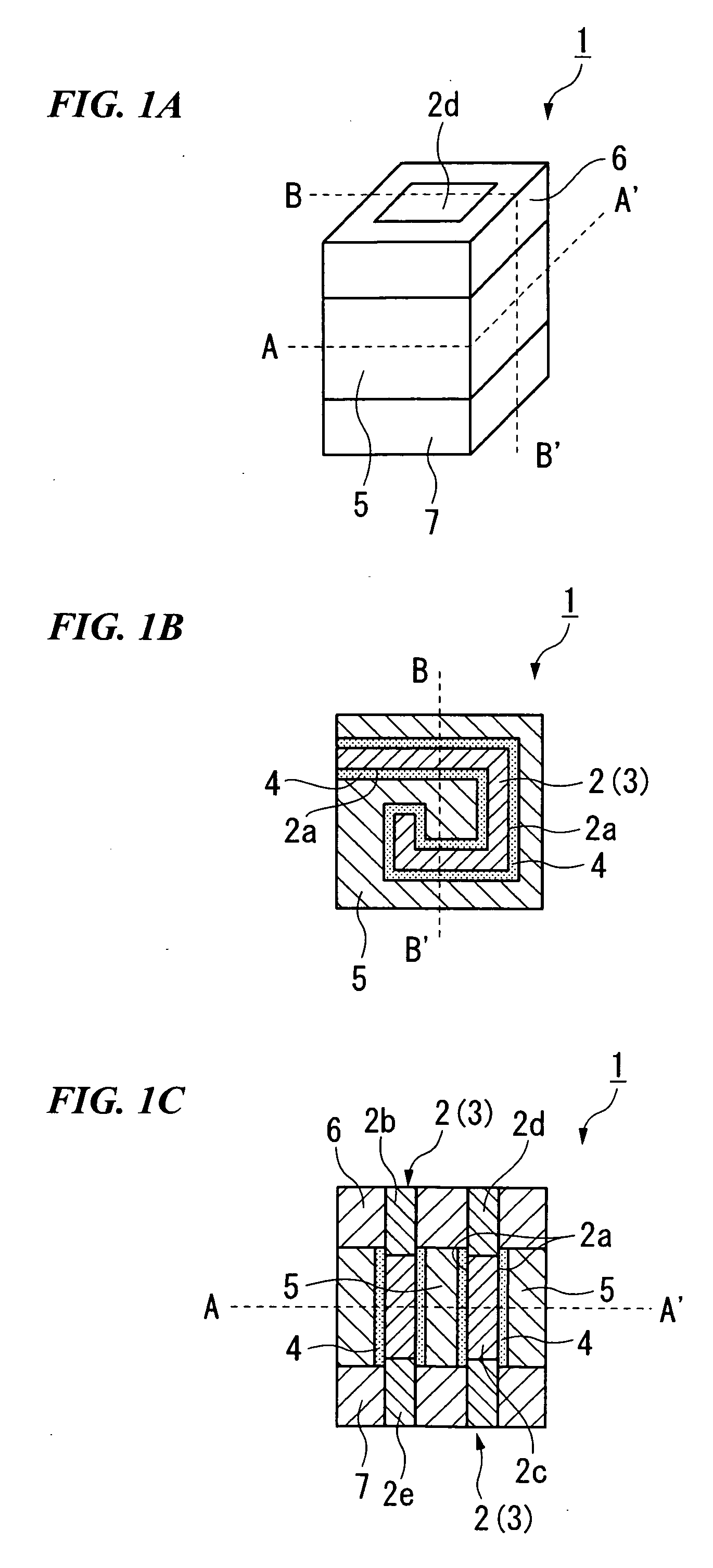
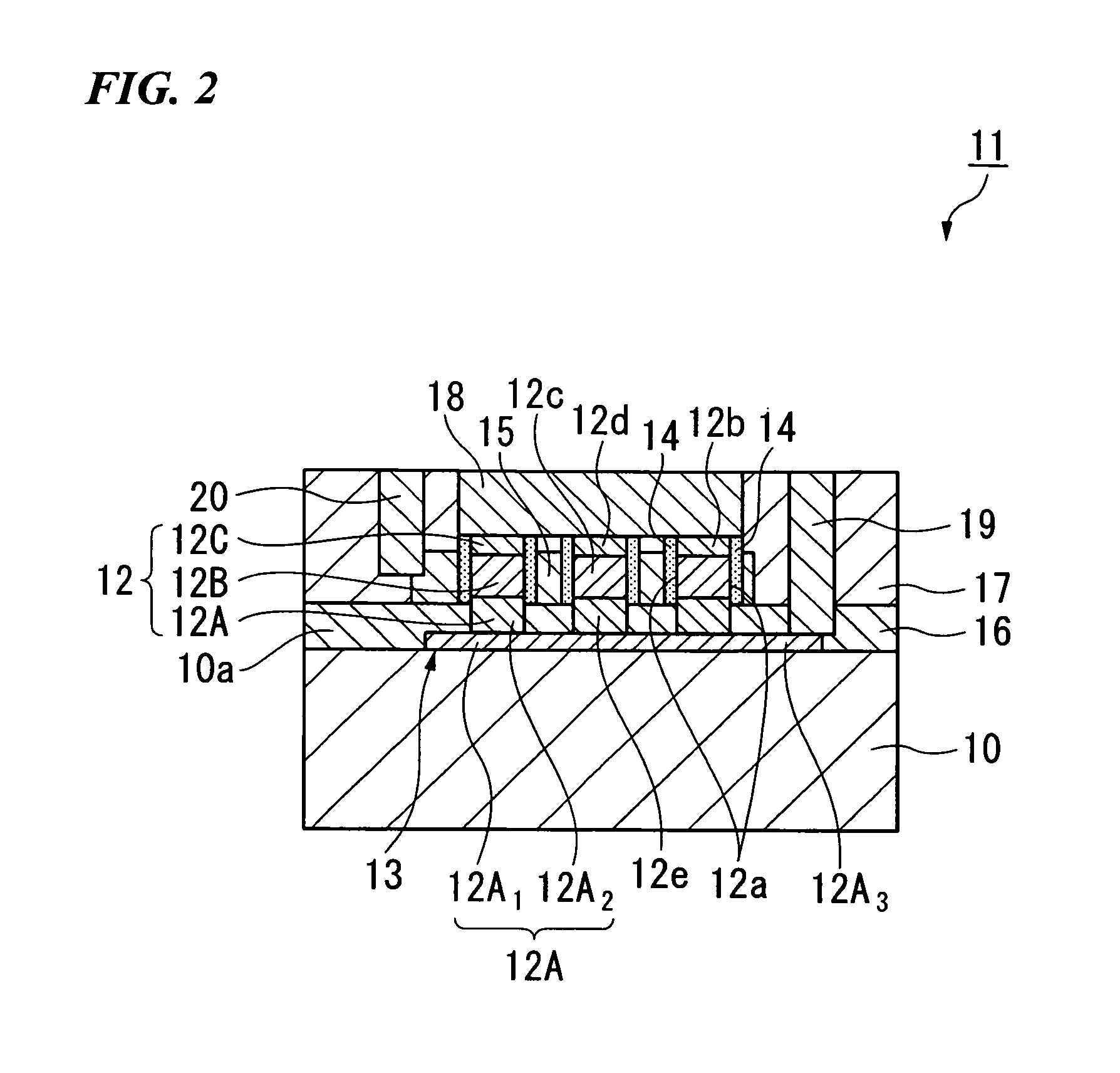
[0102]Hereinafter, a semiconductor device and a method for manufacturing a semiconductor device according to the invention will be described with reference to the accompanying drawings.

[0103]The drawings, which are referred to in the following description, are presented merely for illustration of a semiconductor device or the like of the embodiment, and therefore, the size, thickness, or dimension of each part shown may differ from the actual size, thickness, or dimension of the part in the actual semiconductor device or the like.

Basic Example of Semiconductor Device

[0104]Now referring to FIGS. 1A to 1C, a basic example of a semiconductor device according to the embodiment will be described.

[0105]FIG. 1A is a perspective view of the semiconductor device according to the embodiment.

[0106]Moreover, FIG. 1B is a cross-sectional view taken along the A-A′ line in FIG. 1A, showing the substrate surface of the semiconductor substrate in a plan view.

[0107]Furthermore, FIG. 1C is a cross-sec...


PUM


Abstract

A semiconductor device includes: a semiconductor substrate having a substrate surface; a spiral body constituted by a linear semiconductor layer on which a body region including a channel region, a first source / drain region disposed on the body region, and a second source / drain region disposed under the body region or in the semiconductor substrate around the linear semiconductor layer are formed, the linear semiconductor layer being formed on the substrate surface substantially in a spiral form viewed from the substrate surface in a plan view, formed substantially in a protrudent form in a cross-sectional view, and having a pair of sidewall portions; a gate insulating film formed on at least the pair of sidewall portions constituting the linear semiconductor layer; and a gate electrode that is adjacent to the pair of sidewall portions via the gate insulating film.

Description

BACKGROUND OF THE INVENTION[0001]1. Field of the Invention[0002]The present invention relates to a semiconductor device and a method for manufacturing a semiconductor device.[0003]Priority is claimed on Japanese Patent Application No. 2007-161240, filed Jun. 19, 2007, the content of which is incorporated herein by reference.[0004]2. Description of the Related Art[0005]In recent years, with the rapid development of mobile information communication terminals as represented by cellular phones, the requirements of components mounted thereon, i.e., semiconductor integrated circuits, such as low power consumption and high integration density have become strict.[0006]As an example of a conventional semiconductor device, those disclosed in Japanese Unexamined Patent Application, First Publication No. H05-007003, Japanese Unexamined Patent Application, First Publication No. 2004-039806, and Japanese Unexamined Patent Application, First Publication No. 2005-236290 can be referred to.[0007]For...

Claims


Application Information

Patent Timeline
Patent Type & Authority Applications(United States)
IPC IPC(8): H01L29/78H01L21/336
CPCH01L29/4238H01L29/42384H01L29/42392H01L29/7833H01L29/78642H01L29/78696
Inventor HIGASHINO, TOSHIYUKI
Owner ELPIDA MEMORY INC
Learn More