Pitch by Splitting Bottom Metallization Layer

a technology of metallization layer and bottom metallization layer, which is applied in the direction of semiconductor devices, electrical equipment, semiconductor/solid-state device details, etc., can solve the problems of significant increase in rc delay in the interconnect structure, problems such as gating issues, and increase in copper voids, so as to reduce the resistivity of metal lines and reduce the rc delay. , the effect of the metal line pitch and width

Active Publication Date: 2008-12-25
TAIWAN SEMICON MFG CO LTD
View PDF3 Cites 16 Cited by
  • Summary
  • Abstract
  • Description
  • Claims
  • Application Information

AI Technical Summary

Benefits of technology

[0011]By dividing the bottom metallization layer into a first and a second M1 layer, the pitches and widths of metal lines in the first and the second metallization layers are improved. Accordingly, the resistivity of the metal lines is reduced, and RC delay is reduced.

Problems solved by technology

However, this causes several problems.
Accordingly, the RC delay in the interconnect structure significantly increases.
Second, when copper is filled into via openings and trench openings, copper void will become a major problem.
In 30 nm and 40 nm technologies, these problems have become gating issues.
This is because the width and spacing of metal lines are limited by the dimensions of the underlying integrated circuits.

Method used


Image

  • Pitch by Splitting Bottom Metallization Layer
  • Pitch by Splitting Bottom Metallization Layer
  • Pitch by Splitting Bottom Metallization Layer

Examples


Embodiment Construction

[0015]The making and using of the presently preferred embodiments are discussed in detail below. It should be appreciated, however, that the present invention provides many applicable inventive concepts that can be embodied in a wide variety of specific contexts. The specific embodiments discussed are merely illustrative of specific ways to make and use the invention, and do not limit the scope of the invention.

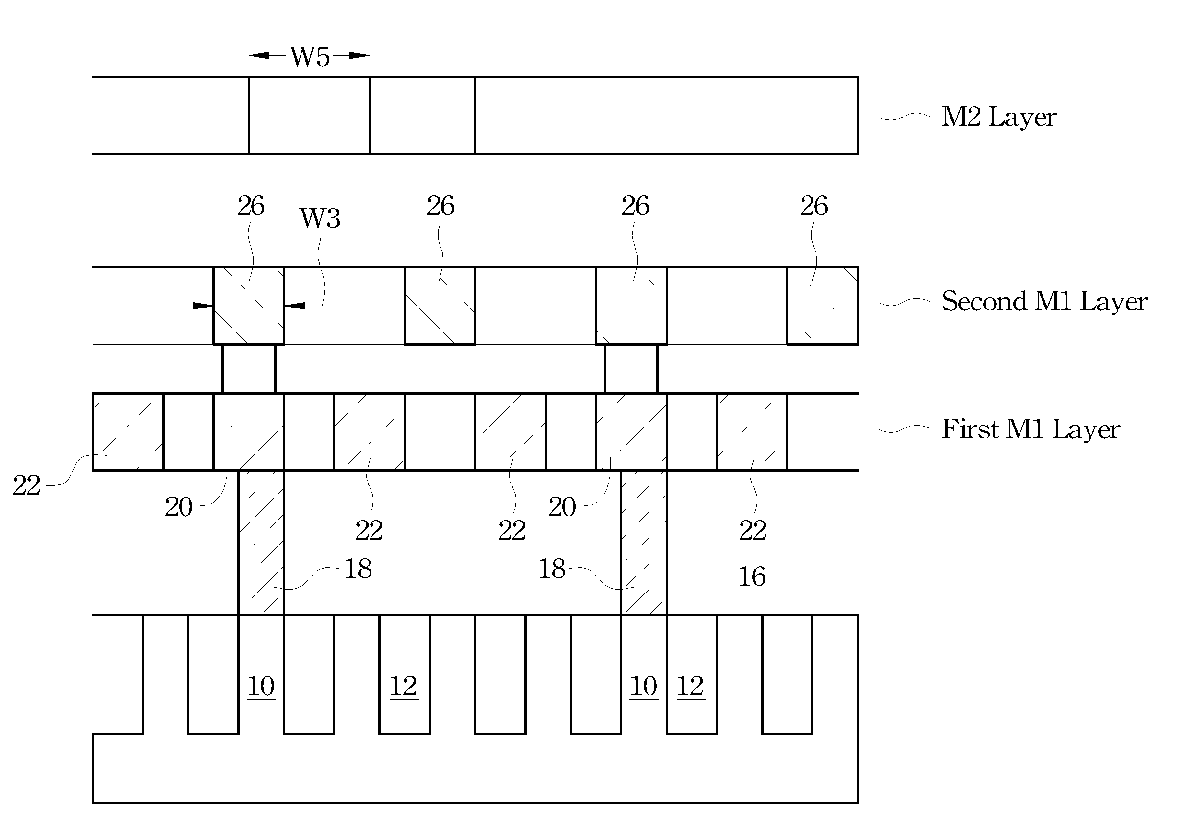
[0016]A novel interconnect structure and methods of forming the same are presented. The intermediate stages of manufacturing a preferred embodiment of the present invention are illustrated. Throughout the various views and illustrative embodiments of the present invention, like reference numbers are used to designate like elements. Throughout the description, a NAND flash memory array and a corresponding overlying interconnect structure are used as examples. However, one skilled in the art will realize that the teaching of the present invention is also applicable to the forma...


PUM


Abstract

An integrated circuit structure includes a semiconductor substrate; a first bottom metallization (M1) layer over the semiconductor substrate; a second M1 layer over the first M1 layer, wherein metal lines in the first and the second M1 layer have widths of greater than about a minimum feature size; and vias connecting the first and the second M1 layers.

Description

TECHNICAL FIELD[0001]This invention relates generally to integrated circuits, and more particularly to the structure and formation processes of metallization layers for connecting the integrated circuits.BACKGROUND[0002]A conventional integrated circuit contains a plurality of metal lines separated by inter-wiring spacings, which metal lines include bus lines, bit lines, word lines, logic interconnect lines, and the like. Typically, the metal lines of vertically spaced metallization layers are electrically interconnected by vias. Metal lines formed in trench-like openings typically extend substantially parallel to the semiconductor substrate. Semiconductor devices of this type, according to current technology, may include eight or more levels of metallization layers in order to satisfy device geometries and micro miniaturization requirements.[0003]FIGS. 1 and 2 illustrate a connection to a conventional NAND flash memory array. Referring to FIG. 1, the array includes a plurality of a...

Claims


Application Information

Patent Timeline
Patent Type & Authority Applications(United States)
IPC IPC(8): H01L23/482H01L29/06
CPCH01L23/522H01L27/0207H01L27/10882H01L27/11517H01L2924/0002H01L2924/3011H01L2924/00H10B12/48H10B41/00
Inventor XU, JEFFREY JUNHAO
Owner TAIWAN SEMICON MFG CO LTD
Why Eureka
Try Eureka