Semiconductor device, method of fabricating the same, stacked module including the same, card including the same, and system including the stacked module

a technology of semiconductor devices and stacked modules, applied in the field of semiconductor devices, can solve the problems of difficult to achieve reliable insulation between pads coupled to chip selection signal lines and other circuits, negatively affecting the integration density of semiconductor devices, and difficult to form plurality of vias or spread plurality of conductive pastes on high-density semiconductor devices. achieve the effect of not reducing the integration thereo

Active Publication Date: 2009-01-01
SAMSUNG ELECTRONICS CO LTD
View PDF2 Cites 14 Cited by
  • Summary
  • Abstract
  • Description
  • Claims
  • Application Information

AI Technical Summary

Benefits of technology

[0008]Example embodiments of the present invention provide a semiconductor device in which a plurality of chips can be reliably stacked without reducing the integration thereof.

Problems solved by technology

However, it is difficult to form a plurality of vias or to spread a plurality of conductive pastes on high-density semiconductor devices evenly without contacting other circuits.
Particularly, allotting an additional area for connecting chip selection signal lines within the semiconductor devices negatively impacts the integration density of the semiconductor devices.
Furthermore, achieving reliable insulation between the pads coupled to the chip selection signal line and other circuits is difficult.

Method used


Image

  • Semiconductor device, method of fabricating the same, stacked module including the same, card including the same, and system including the stacked module
  • Semiconductor device, method of fabricating the same, stacked module including the same, card including the same, and system including the stacked module
  • Semiconductor device, method of fabricating the same, stacked module including the same, card including the same, and system including the stacked module

Examples


Embodiment Construction

[0028]Hereinafter, the present invention will be described more fully with reference to the accompanying drawings, in which preferred embodiments of the invention are shown. This invention may, however, be embodied in many different forms and should not be construed as being limited to the embodiments set forth herein. Rather, these embodiments are provided so that this disclosure will be thorough and complete, and will fully convey the scope of the invention to those skilled in the art. In the drawings, the thickness of layers and regions are exaggerated for clarity.

[0029]In the embodiments of the present invention, a semiconductor device may be provided in the form of a semiconductor chip or a semiconductor package.

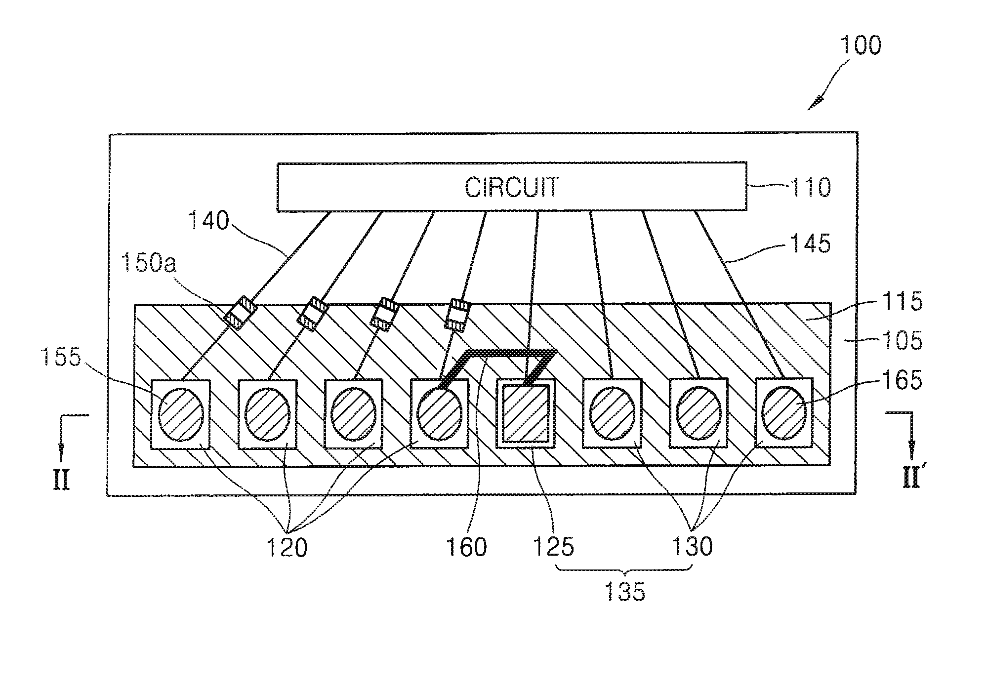
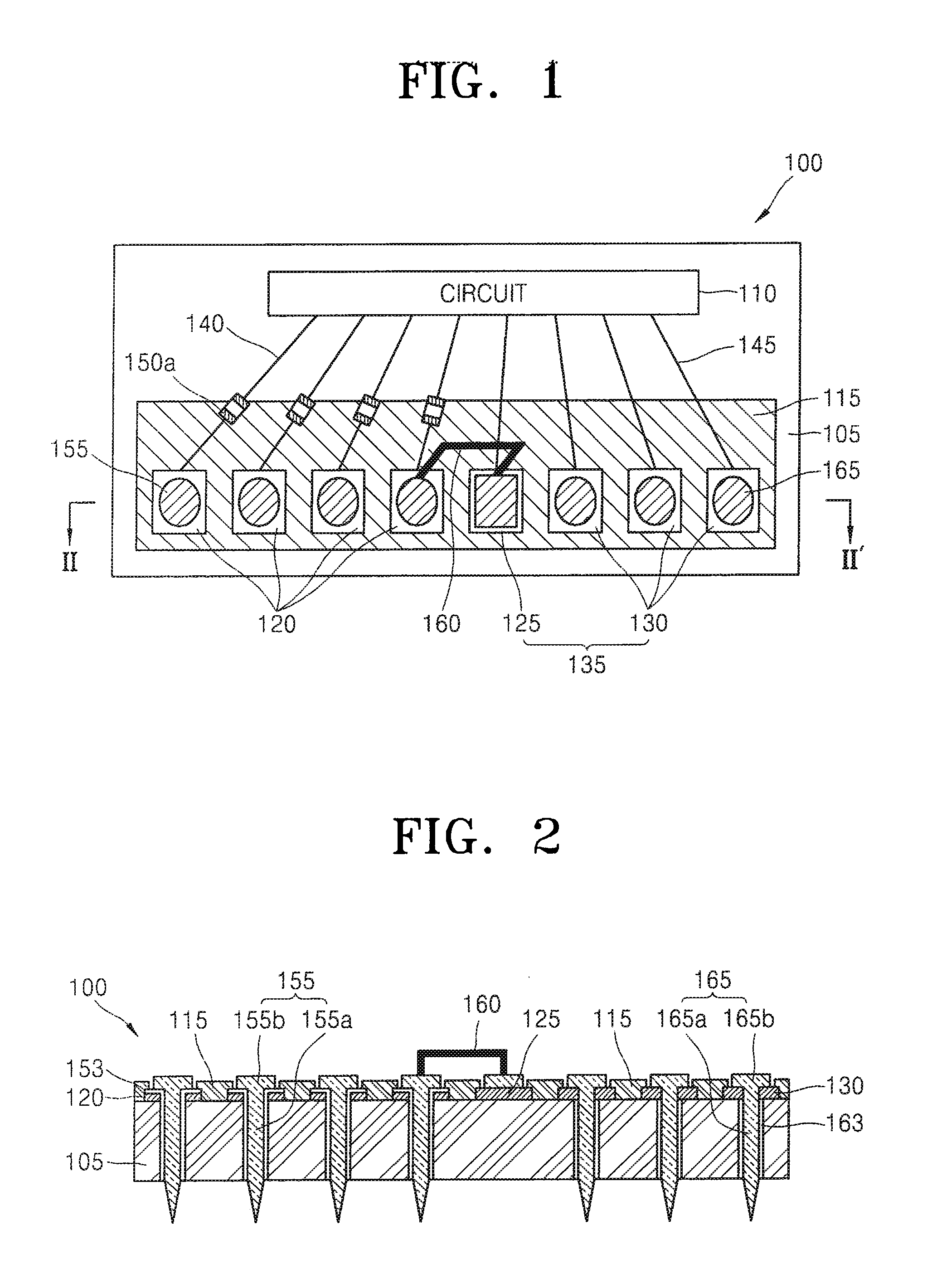
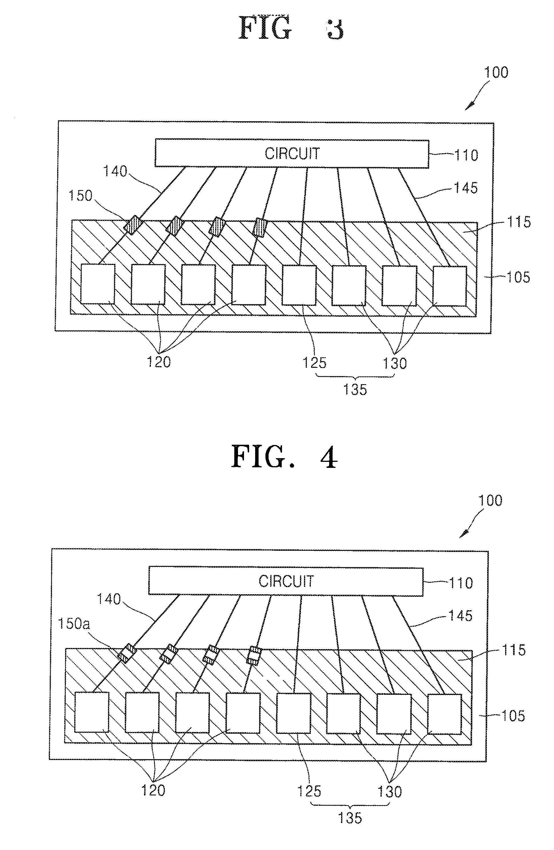
[0030]FIG. 1 is a plan view of a semiconductor device 100 according to an embodiment of the present invention. FIG. 2 is a cross-sectional view of the semiconductor device 100 of FIG. 1 cut along line II-II.

[0031]Referring to FIGS. 1 and 2, a circuit 110 may be provided...


PUM


Abstract

A semiconductor device in which a plurality of chips can be reliably stacked without reducing integration thereof. The semiconductor device includes a substrate on which a circuit is provided. Pads are disposed on the substrate for testing the circuit. At least one terminal is provided on the substrate. First conductors are used to electrically couple the pads and the circuit. Second conductors are used to electrically couple the at least one terminal and the circuit. A switching element is disposed in the middle of the first conductors to control the electrical connection between the pads and the circuit. A plurality of semiconductor devices may be stacked on top of one another to form a stacked module, wherein chip selection lines are formed, which extend to the bottom of each of the semiconductor devices to electrically couple chip selection terminals from among the at least one terminal of the semiconductor devices.

Description

CROSS-REFERENCE TO RELATED PATENT APPLICATION[0001]This application claims the benefit of Korean Patent Application No. 10-2007-0064591, filed on Jun. 28, 2007, in the Korean Intellectual Property Office, the disclosure of which is incorporated herein in its entirety by reference.BACKGROUND OF THE INVENTION[0002]1. Field of the Invention[0003]The present invention relates to a semiconductor device, and more particularly, to a semiconductor device having a switching element installed between a circuit and pads, a stacked module including the semiconductor device, a card including the semiconductor device, and a system which include the stacked module.[0004]2. Description of the Related Art[0005]To satisfy the high integration requirement of semiconductor products, a plurality of semiconductor devices can be stacked in chips or packages. In such a stacked structure, semiconductor devices can be individually selected, or when necessary, can be collectively selected. Chip selection sign...

Claims


Application Information

Patent Timeline
Patent Type & Authority Applications(United States)
IPC IPC(8): H01L23/482
CPCH01L23/481H01L23/5258H01L2924/10253H01L23/5382H01L24/48H01L24/81H01L25/0657H01L2224/4813H01L2224/81801H01L2225/06513H01L2225/06527H01L2225/06541H01L2924/01032H01L2924/01047H01L2924/014H01L2924/01006H01L2924/01033H01L2924/01075H01L2924/01076H01L2924/00H01L2924/00014H01L2224/45099H01L2224/05599H01L23/12H01L23/28
Inventor BAEK, SEUNG-DUKKANG, SUN-WON
Owner SAMSUNG ELECTRONICS CO LTD
Why Eureka
Try Eureka