
Semiconductor memory device

Active Publication Date: 2009-01-01
SK HYNIX INC
View PDF19 Cites 4 Cited by
  • Summary
  • Abstract
  • Description
  • Claims
  • Application Information

AI Technical Summary

Benefits of technology

[0013]Embodiments of the invention are directed to providing a semiconductor memory devic

Problems solved by technology

In the case where pads are provided for respective voltages, there is a problem in that a chip size must be increased due to a number of the pads.

Method used


Image

  • Semiconductor memory device
  • Semiconductor memory device
  • Semiconductor memory device

Examples


Embodiment Construction

[0023]Hereinafter, a semiconductor memory device in accordance with the invention will be described in detail with reference to the accompanying drawings.

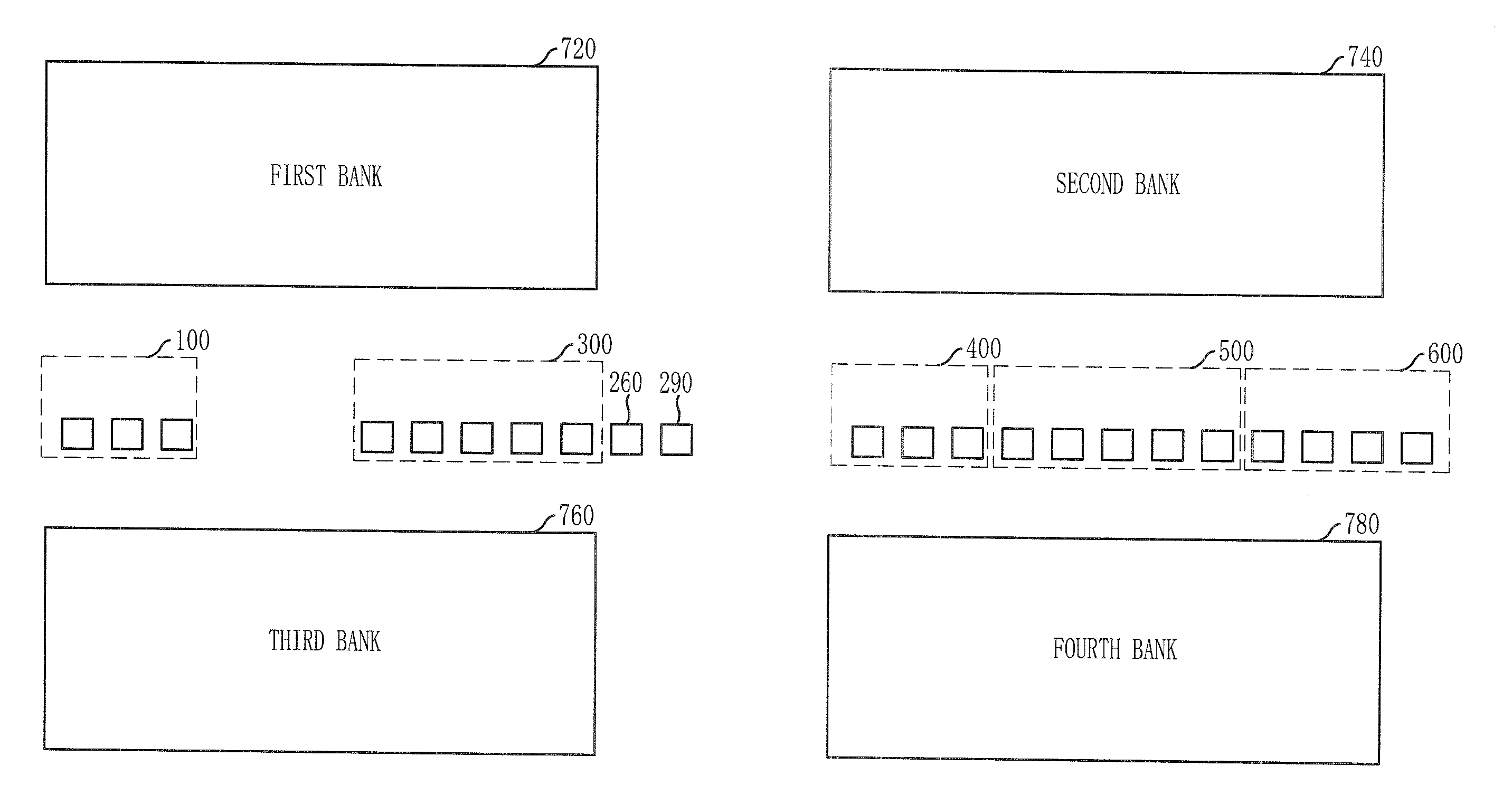
[0024]FIG. 3 is a block diagram illustrating the arrangement of banks and pads in a semiconductor memory device in accordance with an embodiment of the invention.

[0025]Referring to FIG. 3, the semiconductor memory device in accordance with the invention includes zeroth to third banks 720, 740, 760 and 780, a data pad unit 100, a low voltage pad 260, a monitoring pad 290, a reference voltage pad unit 300, a command pad unit 400, an address pad unit 500, and a power supply pad unit 600. In each of the zeroth to third banks 720, 740, 760 and 780, a plurality of unit memory cells for storing data are arranged in an array form. The data pad unit 100 includes a plurality of pads configured to input / output the corresponding data. The low voltage pad 260 is used for inputting / outputting a low voltage. The monitoring pad 290 is provided for...


PUM


Abstract

A semiconductor memory device is capable of measuring internal voltages via a shared pad to reduce a chip size. The semiconductor memory device includes a selector and a monitoring pad. The selector is configured to select one of a plurality of internal signals in response to a test signal and output the selected internal signal. The monitoring pad is configured to output an output signal of the selector to an outside of the semiconductor memory device.

Description

CROSS-REFERENCE TO RELATED APPLICATIONS[0001]The present application claims priority to Korean patent application number 10-2007-0063718, filed on Jun. 27, 2007, which is incorporated by reference in its entirety.BACKGROUND OF THE INVENTION[0002]The present invention relates to semiconductor design technology, and more particularly to a pad of a semiconductor memory device for inputting / outputting a signal.[0003]In general, semiconductor memory devices include contacts, e.g., pads, for inputting or outputting a variety of signals. Semiconductor memory devices must have predetermined number of pads at least that corresponds to number of kinds of various signals and external supply voltages, which are defined in a standard spec. Besides, semiconductor memory devices further include additional pads for a testing procedure generally. Thus, the additional pads are used for monitoring internally generated voltages of a semiconductor device or applying internal signals from the outside.[00...

Claims


Application Information

Patent Timeline
IPC IPC(8): G11C5/14G11C29/00
CPCG11C29/021G11C29/48G11C29/1201G11C7/12G11C8/08G11C8/10G11C2207/105
Inventor KANG, KHIL-OHK
Owner SK HYNIX INC
Learn More